Back Drilling PCB Capabilities
Advanced PCB manufacturing with OurPCB’s back drilling capabilities, which remove copper stubs from multilayer boards to improve signal integrity and minimize distortion.


Why is Back Drill PCB Needed?
Back drill PCB is needed to remove non-functional via stubs that cause signal reflections, distortion, and EMI in high-speed multilayer circuit boards. By eliminating these stubs, back drilling improves signal integrity, reduces bit error rates, and enables higher data transmission speeds in advanced electronic applications.
PCB Manufacturing Process


Factors That Influence the Effectiveness of Back Drilling
FR4 is the most common material used to build PCBs and it is fairly easy to drill regardless of its thickness. But high-performance circuit boards built using metal (metal cores) and ceramic have some drilling challenges because the materials are relatively tougher than FR4. These materials are more thermally conductive as well, so you’ll need different drilling parameters and bits to get the job done.
Small vias spaced close to each other require tiny drill bits to conduct more precise drilling, but large vias with more spacing in between give you more leeway. But you’ll need a larger drill bit and possibly do multiple passes to eliminate the unwanted copper and substrate materials. Read more about PCB Via sizes.
While backdrilling, it is important to avoid damaging the board by drilling through the copper power/ground planes and transmission lines. Suppose the clearance between these components and the drill bit is too narrow. In that case, it might be better to avoid backdrilling, use an extremely tiny drill bit with utmost precision, or avoid mechanical drilling. Laser and plasma drilling options are more accurate.
How Much Residual Stub Can Remain After Backdrilling?
| Residual Stub Length | Approximate Signal Loss |
|---|---|
| 1 mil | 0.25% |
| 2 mils | 0.5% |
| 5 mils | 1.25% |
| 10 mils | 2.5% |
| 20 mils | 5% |
| 40 mils | 10% |
| 60 mils | 15% |
| 100 mils | 25% |
| 200 mils | 50% |
When you decide to backdrill your multilayer PCB, you must determine how far you’ll dig in or the stub length you want to remain. Determining this value depends on several factors, but the key one is signal integrity.
The longer the stub length that remains, the higher the signal loss, so the shorter it is, the better. Here’s a breakdown of how to determine the residual stub to leave behind based on the signal loss.
Back Drill Table with
Design Values
| Types | Value min. |
|---|---|
| Back drilling Ø | 400 μm |
| Plated-through via Ø | 200 μm |
| Copper clearance | 150 μm |
| Ø-Difference circumference | 100 μm |
| Back drilling depth | 200 μm |
| Distance to connected layer | See below |
| Thickness target layer | See below |
| Thickness stub remainder (safety) | See below |
Required Target layer
Thickness “G”
| F ≤ 1.0 mm | 1.0 mm < F ≤ 2.0 mm | 2.0 < F ≤ 3.0 mm | 3.0 < F ≤ 4.0 mm | |
|---|---|---|---|---|
| G min. | 250 μm | 300 μm | 400 μm | 500 μm |
| H | 125 μm | 150 μm | 200 μm | 250 μm |
| Tolerance | ±100 μm | ±125 μm | ±175 μm | ±225 μm |
Key
Gmin. = Thickness Target Layer.
H = Distance To Connected Layer.
Tolerance = Thickness Stub Remainder.
PCB Assembly Services

We handle everything from parts sourcing to final assembly, providing a hassle-free experience that ensures top-quality boards every time.

Whether you need a few prototypes or large-volume batches, our flexible assembly services adapt to your project’s scope and timeline.

Stay environmentally responsible with our compliant assembly processes, offering RoHS and lead-free options for safe, reliable builds.

No matter the complexity, we can assemble boards of all configurations—single-layer, multi-layer, or a mix—to match your exact specifications.

From one-off prototypes to bulk orders, we accommodate projects of all sizes without compromising on quality or turnaround time.

Join our growing community of satisfied clients who rely on our dependable assembly expertise and dedicated customer support.
Millions of business and innovators use OurPCB


PCB Board Process
Order Received
- Component Procurement
- Preparation
- PCB Manufacture
- Make Process Flow
Soldering
- Solder Printing/Wave Soldering
- SMT/Plugging
- Inspection (repair if necessary)
- AOI (repair if necessary)
- Transfer
Parts Assembly
- Manual Assembly
- Cleaning
- Wire Screw
- Inspection
- Repair If Necessary
Finalization
- Final Confirmation
- Packing
- Shiping
Technical Capabilities
Capabilities & Services
- One-stop PCBA Services (PCB Manufacturing + Components Sourcing + Assembly)
- SMT Assembly + THT Assembly, Single/double-sided Assembly Mixed PCB Assembly
- BGA Rework
- 60,000 Chips/Hour
- Down to 01005/0210 Size
- Accuracy<±40μm
- Min. QFN Pin Width/Space: 0.15mm/0.25mm
- Min. BGA Diameter/Space: 0.2mm/0.35mm
- Rigid, Flex, HDI, & High-speed Power Boards
- Up to 64 Layers
- 60GHz High Frequencies
- Min. Trace Width/Spacing: 1.8mil/1.8mil
- AOI, X-ray, ICT & FCT Testing
- Controlled Impedance
- ISO 9001, ISO 13485, ISO 14001, IATF 16949, IPC-A-610, UL Certified
- Automotive, Medical, & Military-grade PCBA Manufacturing
Steps for a Back Drill
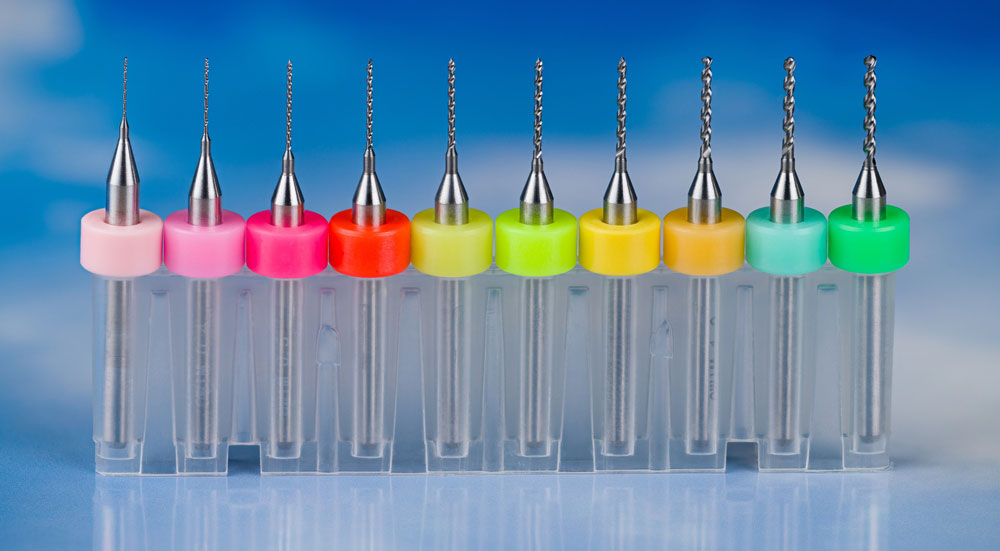
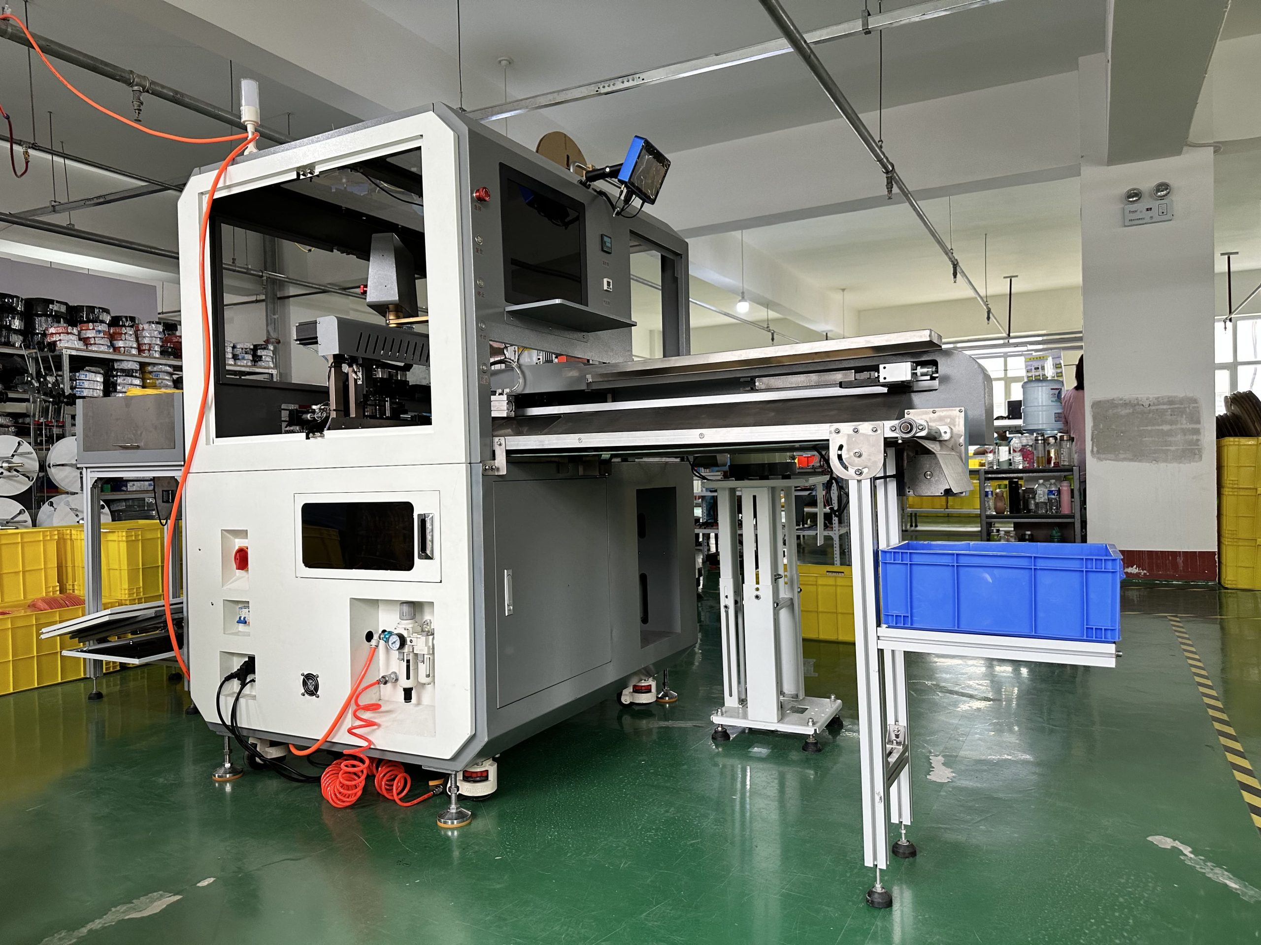
Here are the back-drilling steps you need to follow in the manufacturing process of a PCB:
- Locate the first drilling holes using the positioning holes provided on the PCB.
- Place a dry film to seal the positioning holes before electroplating.
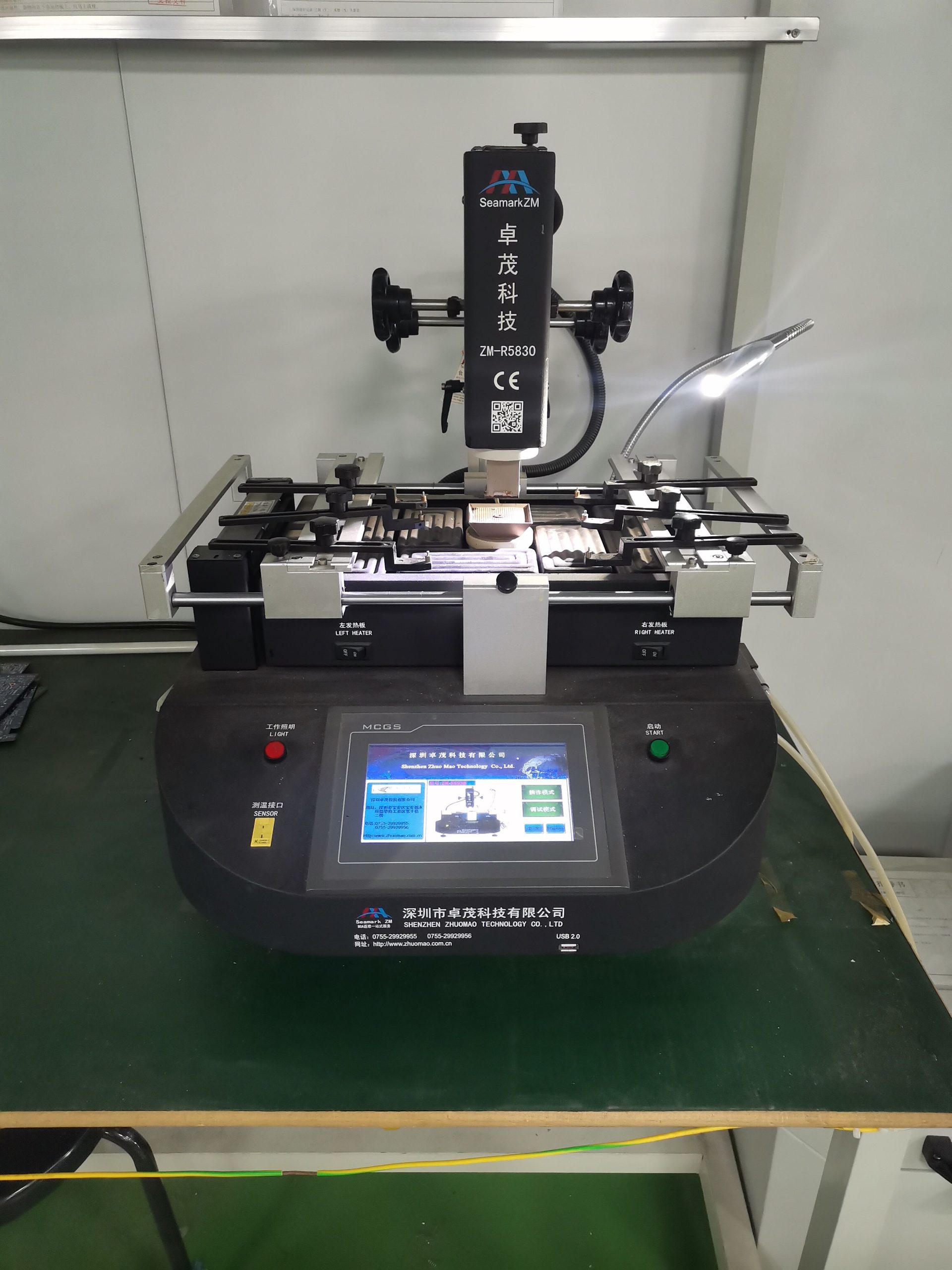
- Electroplate the first drilled PCB board layer.
- Transfer outer layer graphics on the electroplated PCB.
- Once there is an outer layer pattern, perform graphic plating on the PCB.
- Ensure dry film sealing treatment on the positioning hole before graphic plating.
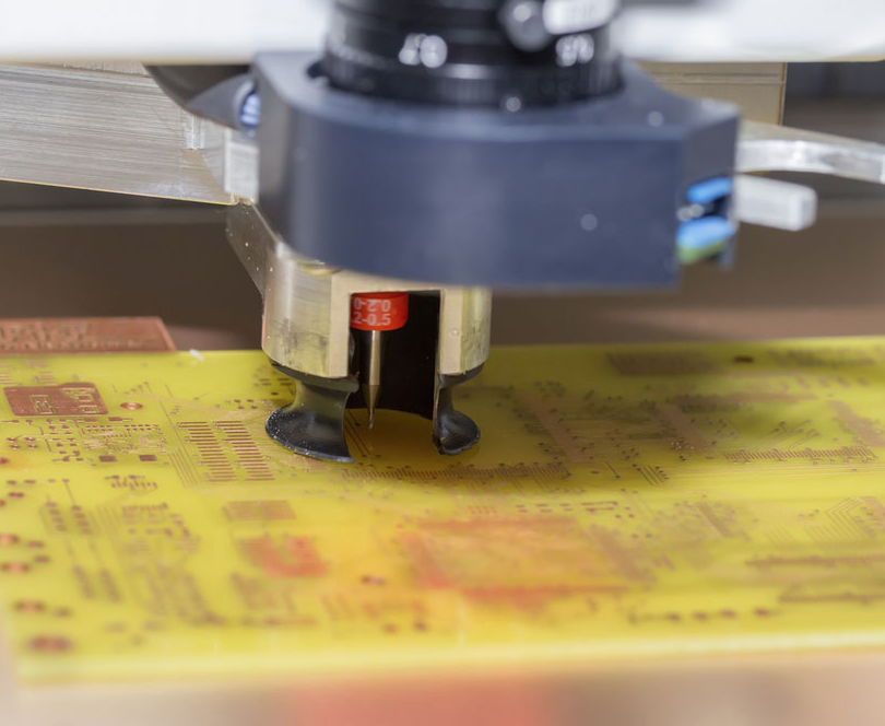
- Use the same positioning hole for the first drill for back drilling.
- Back-drill the electroplated holes that need drilling.
- Clean the back drilling holes properly to eradicate residual drill chips in the back drilling.
Difficulties of Back Drilling Process
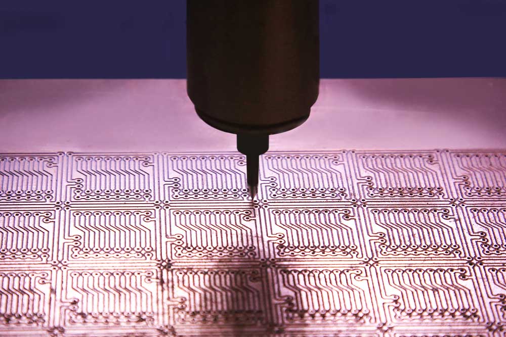
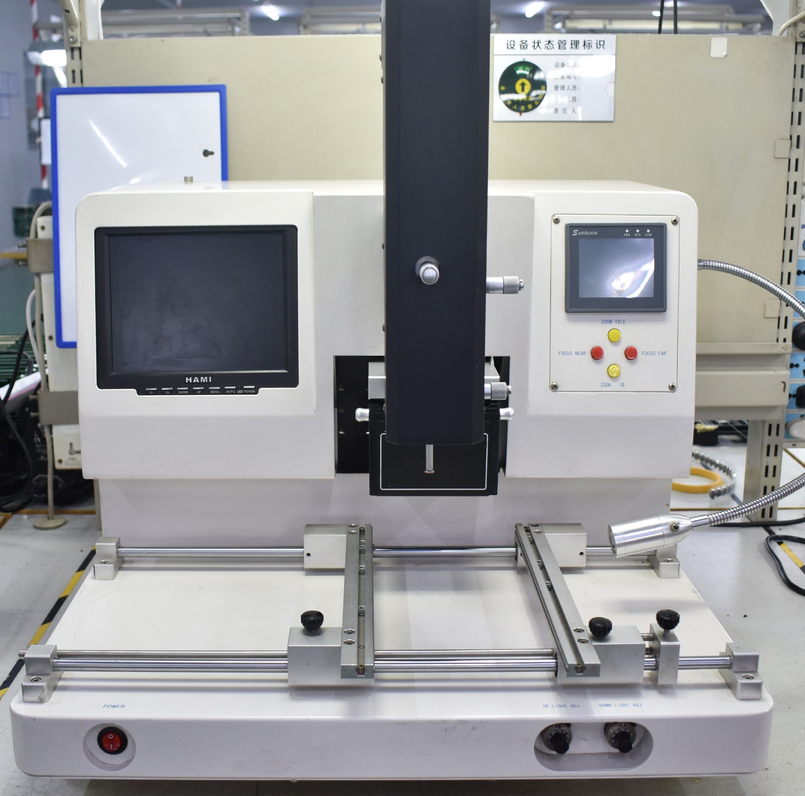
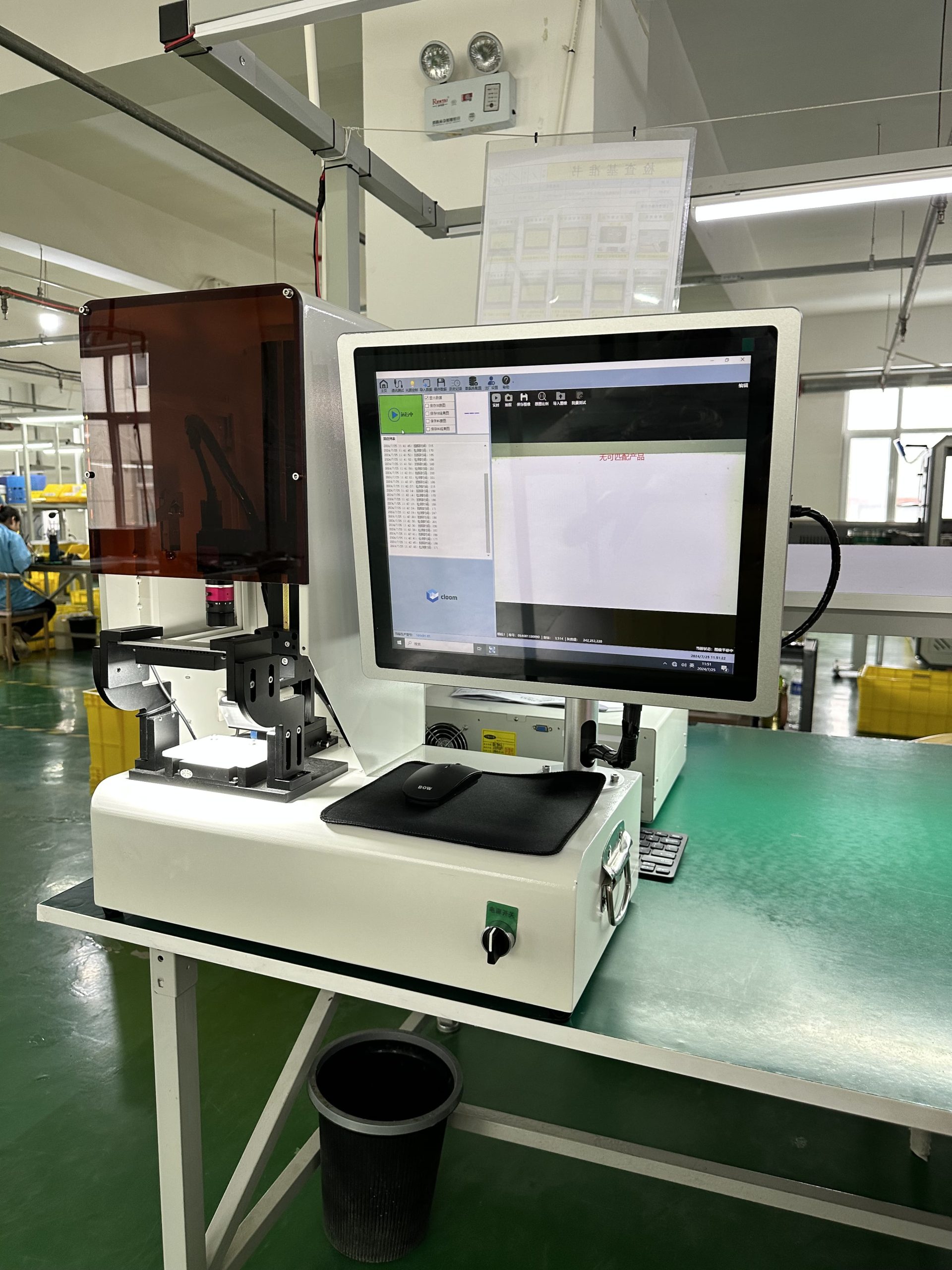
Back Drilling Depth Control
Utilizing the depth control function of the drill to process the blind vias is essential to back drilling. Usually, the tolerance relies on the accuracy and the tolerance of the medium thickness of the equipment.
Also, accuracy depends on external factors like the drill’s resistance, the drill bit’s angle, etc. For this reason, selecting suitable drilling materials and methods is vital to achieving accurate control. In turn, you achieve better results.
Back Drill Accuracy Control
Ultimately, back drilling depends on the hole diameter of the primary drill. This feature makes the accuracy of the secondary drilling coincidence vital. Therefore, it affects the quality control of the PCB going forward.
Also, note the essential design rules like board expansion and contraction, drilling equipment accuracy, drilling methods, etc., before commencing the back drill.
Applications of Back Drilling
The primary purpose of PCB back drilling is to eliminate signal integrity issues caused by non-functional via stubs, which makes it common in high-frequency, radio-frequency, and microwave PCBs that can experience signal losses due to such issues.
Back drilling is also important in complex multilayer PCBs that have over 20 layers, high-speed digital boards that have multi-gigabit data channels, HDI boards, RAM memory routing (DDR3 and DDR4), network switching equipment, servers, telecommunication equipment, etc.
Basically, all modern devices that handle high-speed, high-frequency transmission and have multiple layers (8+) require backdrilling if they have signal-reflecting plated through holes to prevent EMI and signal losses.

Mon-Fri: 24 hours,
Sat: 9am-6pm, GMT+8

Reach us at
[email protected]
24 hours online

+86-199-30589219
Mon-Fri: 24 hours,
Sat: 9am-6pm, GMT+8
FAQ's
What does back drilling involve, how much extra does it cost, and why should I consider it?
Back drilling is a secondary machining step performed after the plated-through holes have been created on a PCB, where an additional drill pass removes the unused copper “stub” on the far side. This process typically adds up to 20% more in manufacturing costs. Despite the extra expense, removing the stub delivers noticeable performance benefits: it improves signal integrity by reducing reflections and insertion loss on high-speed traces, lowers electromagnetic interference by eliminating an unintended antenna, and frees up board real estate to support tighter routing and higher layout density. In many high-speed or densely packed designs, these gains in electrical performance and reliability make back drilling a cost-effective choice.
Why is Back drill also called control depth drilling?
It is because a back drill requires specific calculations. Hence, it achieves the depth necessary for accurate results during the drill.
How much should the dielectric thickness design be?
The ideal dielectric thickness design is at least 0.2mm.
Most Effective Alternatives To Back Drilling
The most effective alternatives are buried and blind vias, where the buried via interconnects the board’s internal layers without being exposed to the outside.
What’s the difference between back drilling and blind vias
Blind vias connect an outer layer to one or more inner layers without going all the way through the board. Back drilling starts with a plated-through via and then removes the unwanted copper “stub” on the far side.
Advantages of blind vias over back-drilled holes
- Signal integrity & EMI
- No residual copper stub → fewer reflections, lower signal loss and reduced electromagnetic interference.
- Cost & reliability
- Eliminates the extra drilling step required for back drilling.
- Reduces the risk of mechanical damage during manufacturing.