


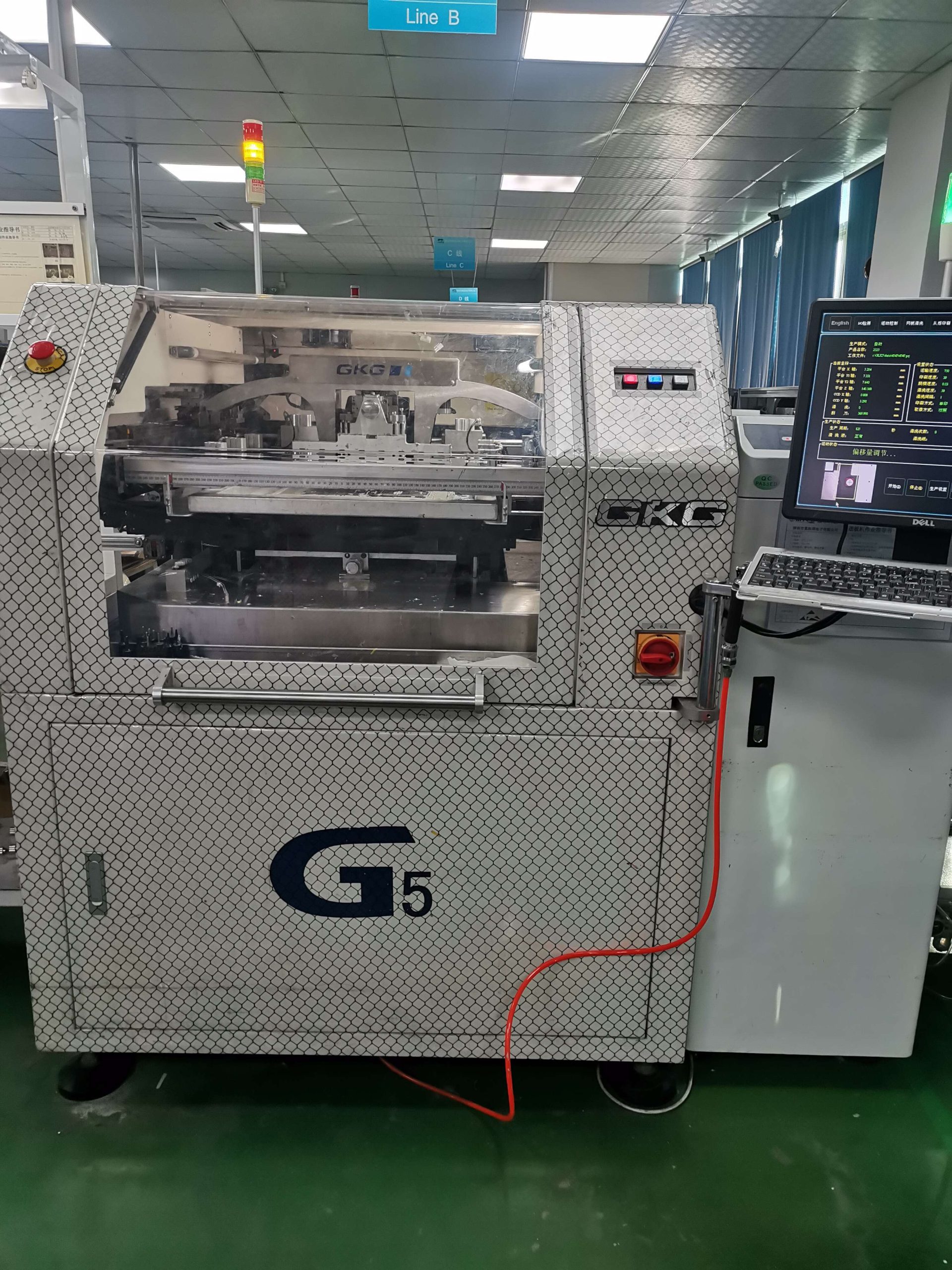
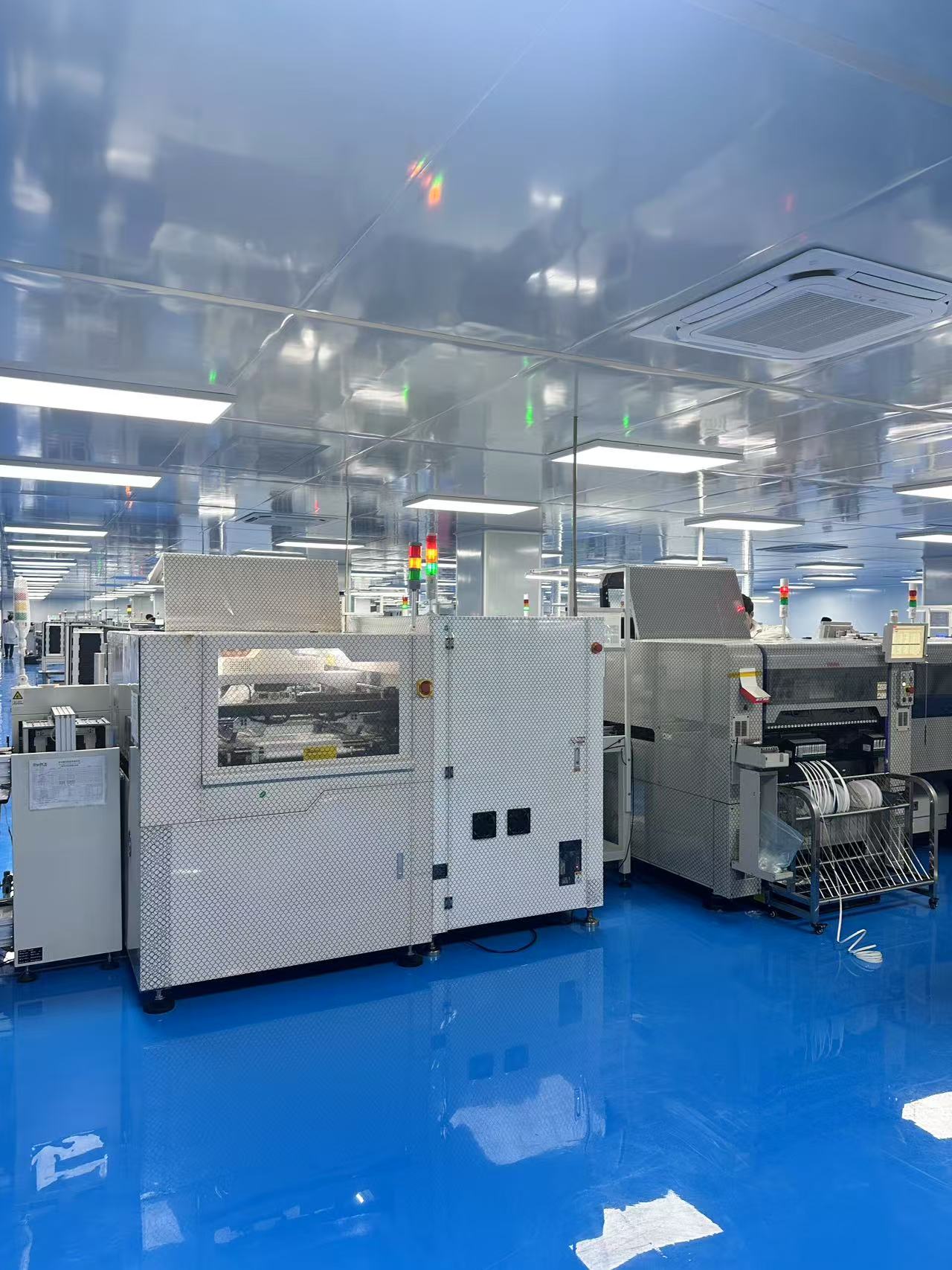
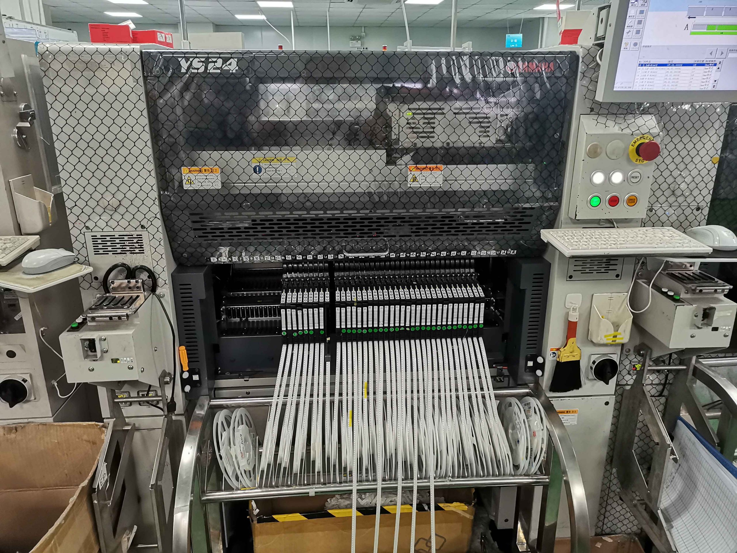
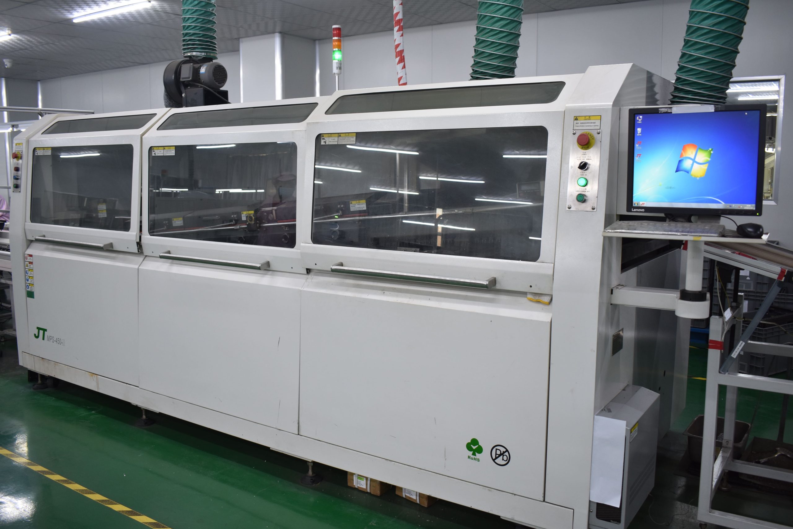
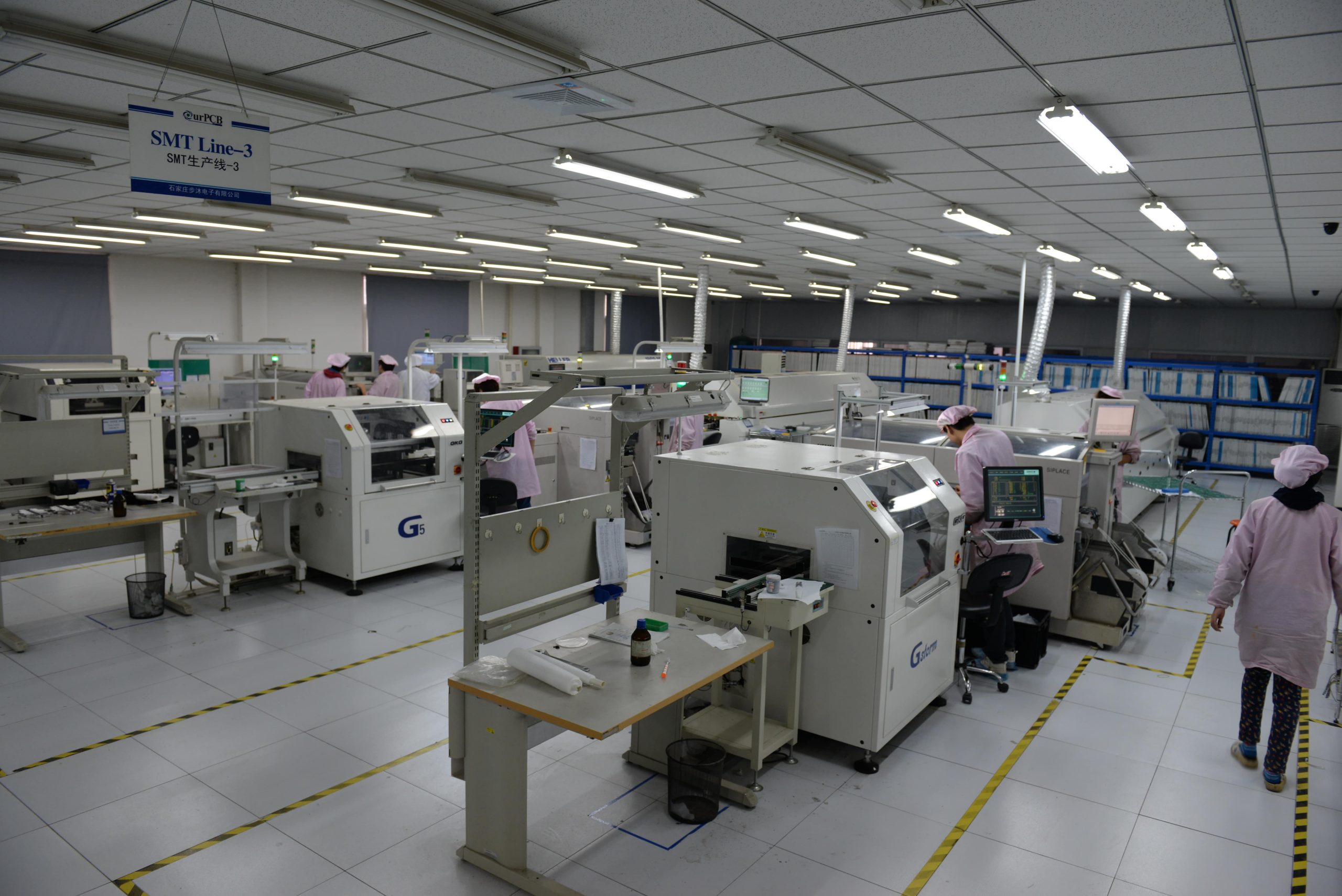
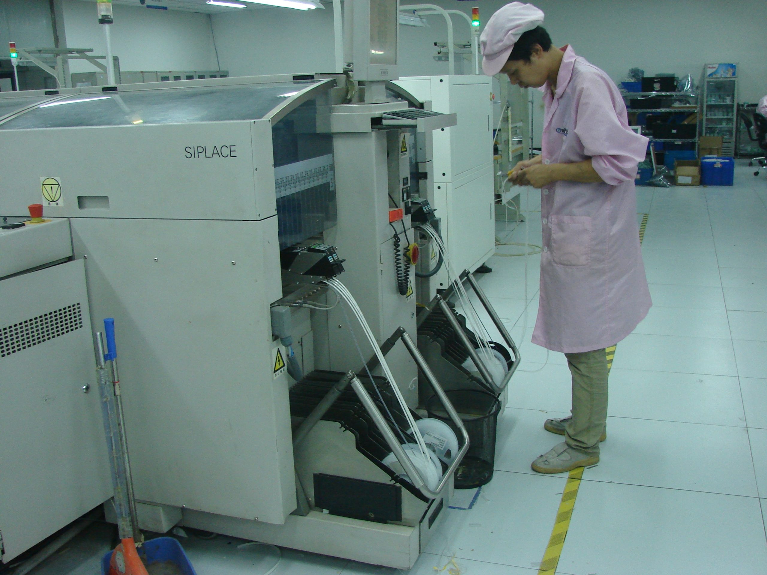
Our two factories in Shenzhen and Shijiazhuang run dedicated SMT lines for fine-pitch work, each with ±25 µm placement accuracy. Climate-controlled rooms and anti-static handling protect 0201 passives and µBGA packages during placement and reflow.

We’re certified to ISO 9001, IATF 16949, and IPC-A-610 Class 2 and Class 3. That means your boards meet the workmanship standards required for medical, aerospace, and automotive programs — no separate audit needed when you scale to volume.

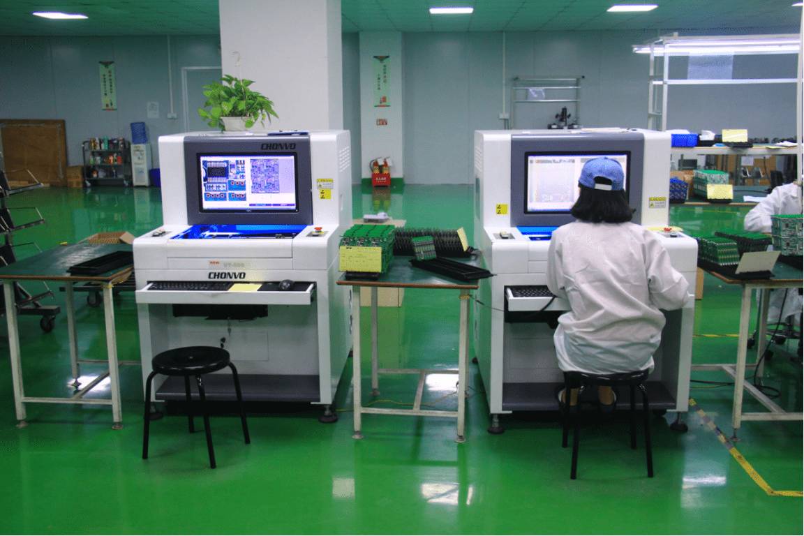
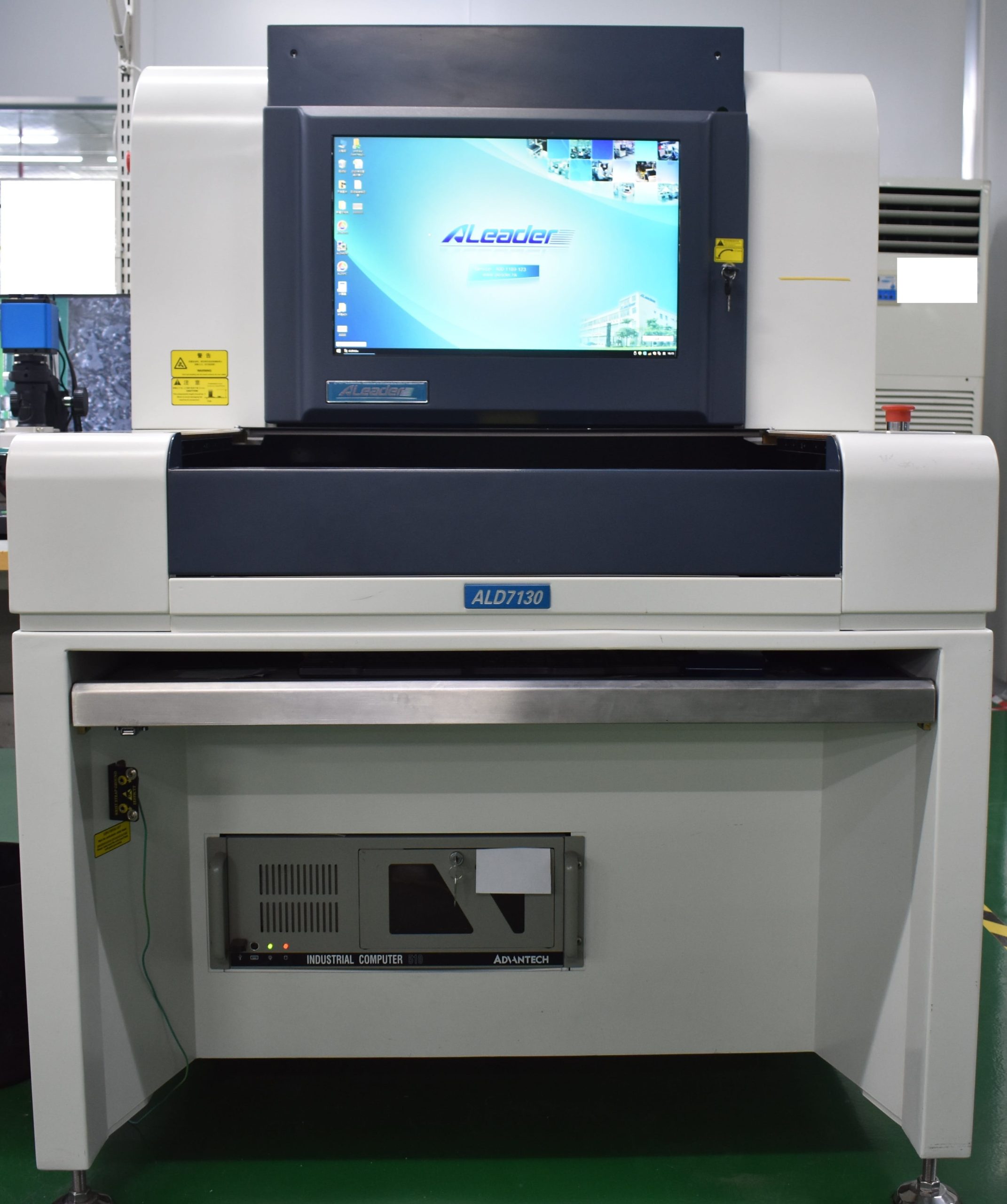
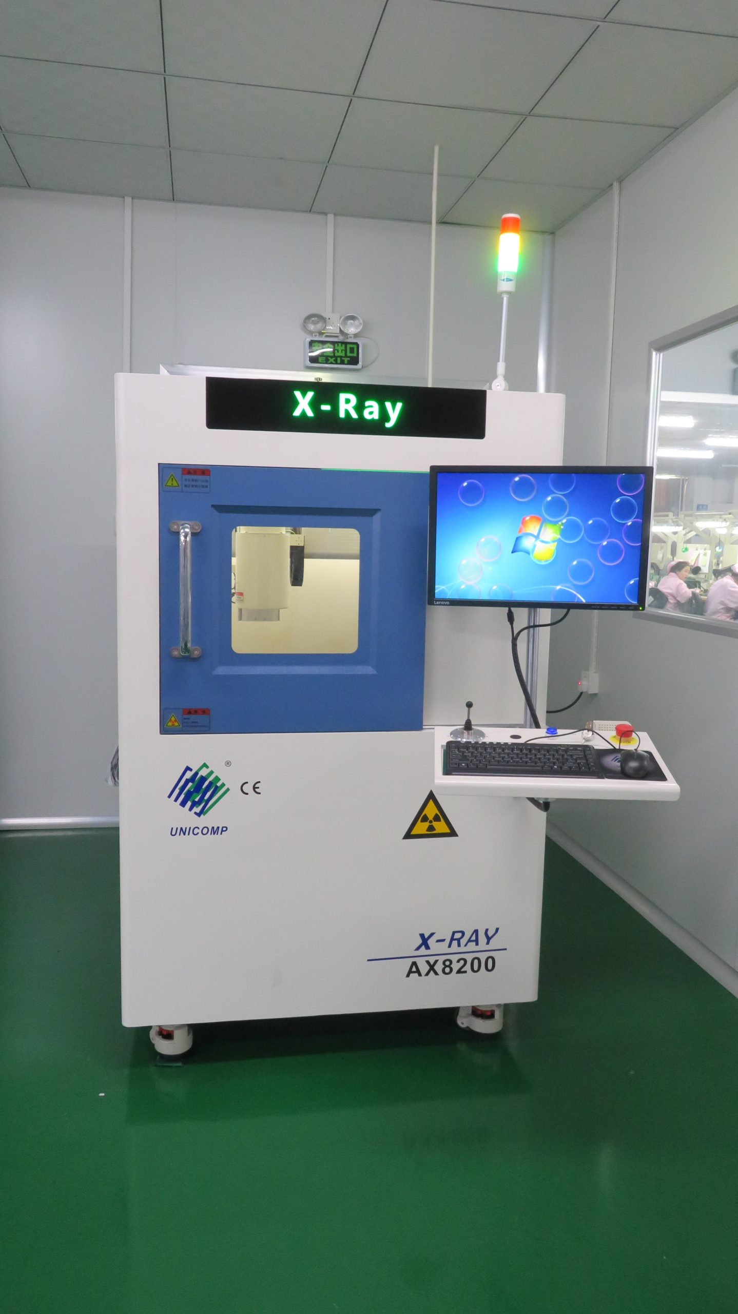
Hidden joints under BGAs and QFNs are inspected with 5-axis X-ray at 2.5 µm/pixel, and every solder fillet is checked by 3D AOI at 15 µm lateral resolution. You get full inspection coverage on every board, not just first-article samples.

Our engineers review your Gerbers, BOM, and stack-up before quoting — flagging pad geometry, via-in-pad, and stencil aperture issues before they hit the line. You’ll know about yield risks while there’s still time to fix them in design.

We source from Digi-Key, Mouser, Arrow, and Future Electronics with full traceability. Moisture-sensitive components are dry-baked, vacuum-sealed, and tracked by MSL level so reflow doesn’t pop a BGA you waited six weeks for.

Standard turnkey PCBA quotes go out in 48 hours; bare-board quotes in 8. Once you approve, fine-pitch prototypes typically ship in 7 to 10 days so you can validate your design before committing to production tooling.
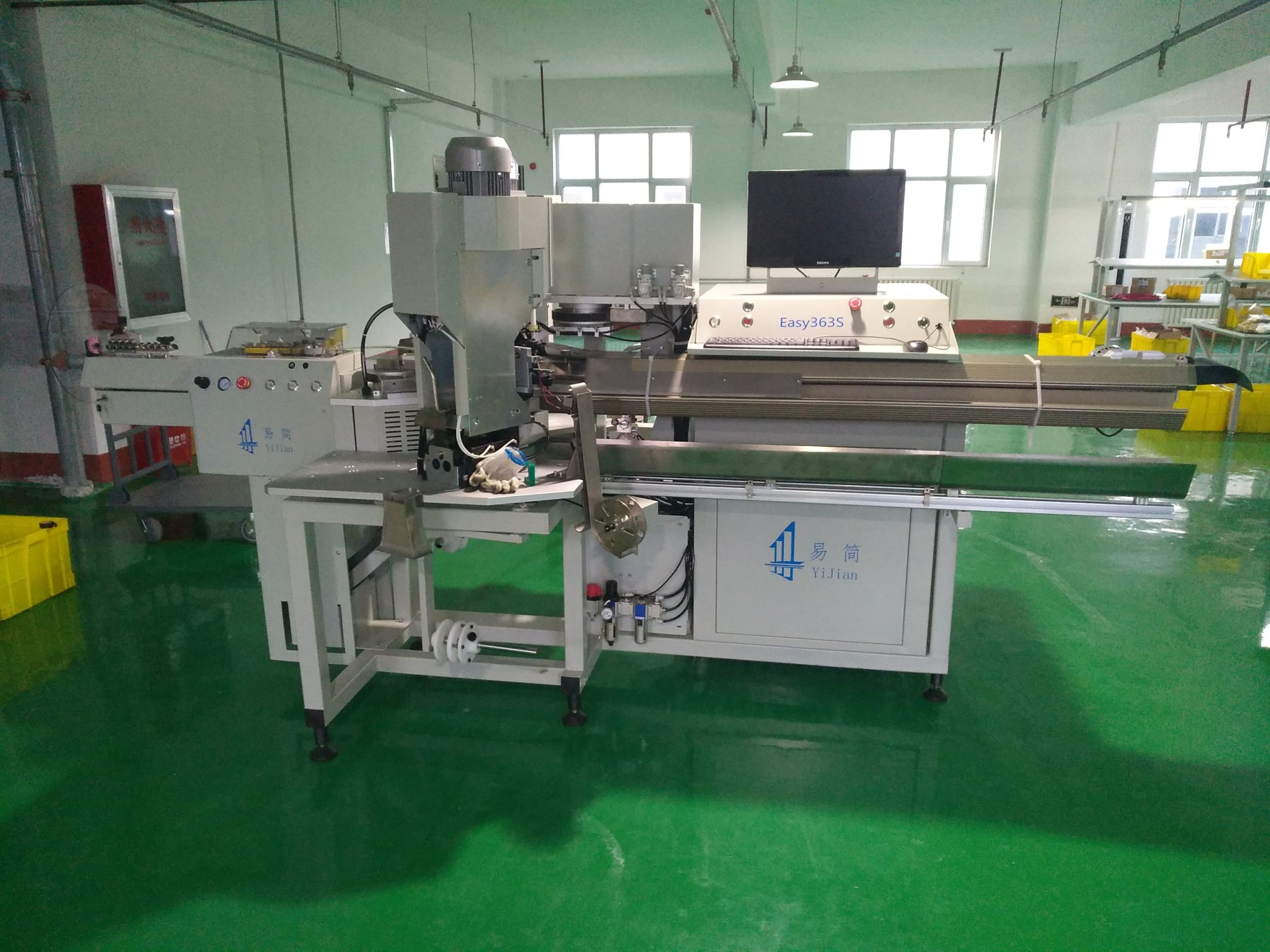
Factory-Ready for Ultra-Fine Assembly
Our dual 10,000 m² PCB assembly houses in Shenzhen and Shijiazhuang are equipped with high-speed SMT assembly lines capable of placing fine-pitch parts with ±25 µm tolerance.
Each line includes temperature- and humidity-controlled environments, active anti-static systems, and vacuum transport for handling thin or flex printed circuits.
Certified for High-Reliability Fine-Pitch Workflows
We are fully certified to ISO 9001, IATF 16949, and IPC-A-610 Class 2 & 3, supporting applications where fine-pitch PCB assembly must meet elevated acceptance criteria for solder joint geometry, lead coplanarity, and component body clearance.
Our QA workflows are built to handle fine-pitch PCBs requiring zero solder bridging and uniform joint fillets across dense arrays.
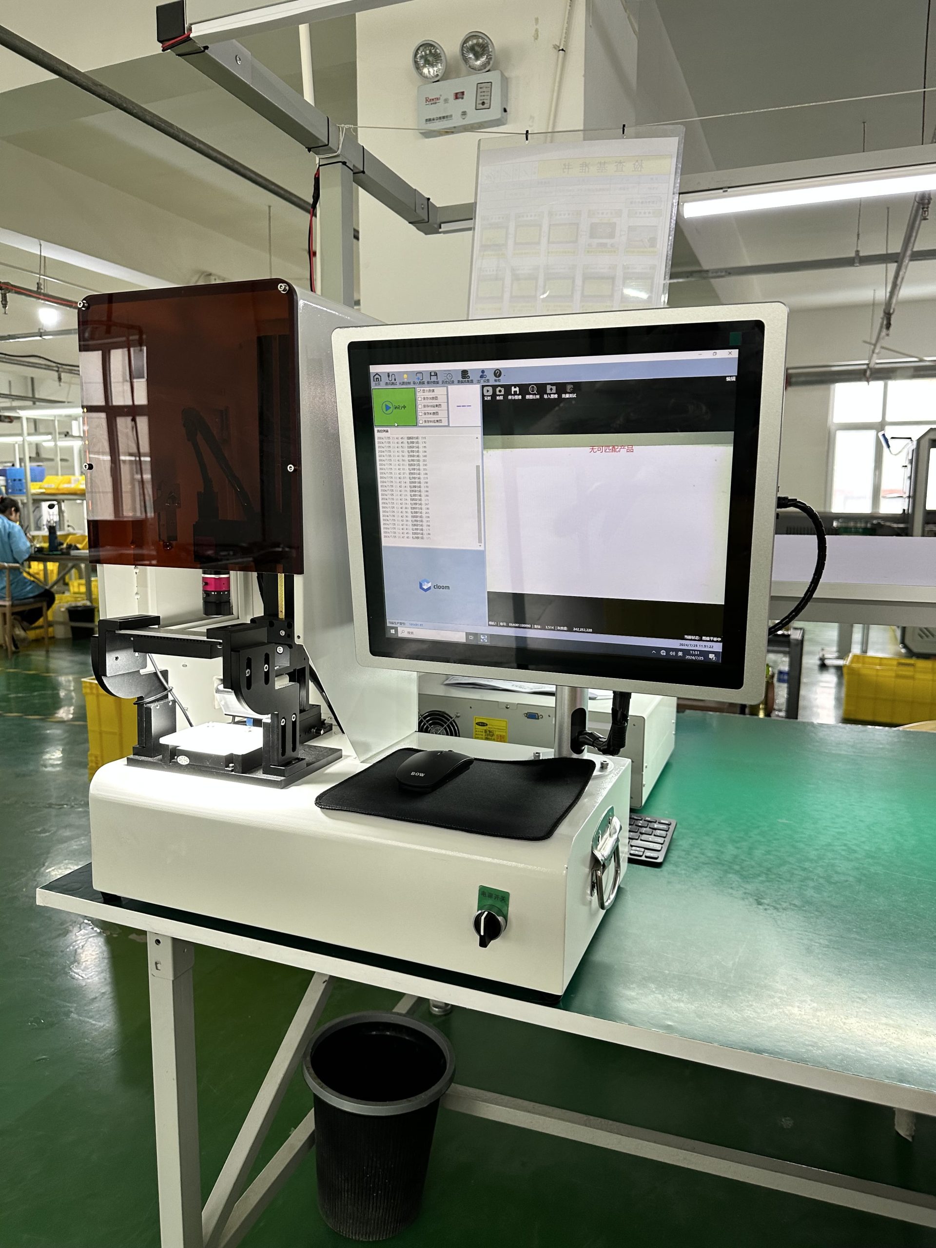
Inspection Systems for High Pin Count Devices
All assemblies involving ball pitch under 0.5 mm, QFN, or PoP packages undergo X-ray inspection, SPI, and AOI with 15 µm resolution optics.
We detect voids, open leads, insufficient solder, lifted terminations, and hidden shorts. This inspection process is a requirement for successful assembly when working with components that provide no visible solder access.
Engineering Review for Pitch-Specific Risks
Every fine-pitch electronic assembly receives a DFM and DFA review focused on stencil coverage, aperture tuning, pcb design limitations, and routing near fine-pitch ICs.
We assist in verifying pad design, thermal pad exposure, and via escape planning, important for high I/O packages like BGA and chip scale layouts where misalignment or solder blockage can compromise yield.
Turnkey Component Sourcing and Lot Control
We offer full assembly component sourcing through partners like Digi-Key, Mouser, and WPG, including traceable lots for hard-to-find or moisture-sensitive electronic components.
Components are stored under MSL-compliant conditions, with drying cabinets and vacuum packaging for all incoming fine-pitch parts.
Fine pitch PCB assembly shows up wherever you need more capability in less space — and where a missed solder joint costs more than the board. Below are the four sectors that drive most of our fine-pitch volume.

Medical electronics and wearables
Diagnostic monitors, implantables, and portable imaging gear use fine-pitch parts to fit sensors, MCUs, and memory into tight spaces. We build these to IPC Class 3 with full traceability per unit barcode.

Consumer electronics and IoT
Phones, tablets, and IoT nodes pack PoP, µBGA, and high-density QFN into dual-sided builds. We support embedded antennas, shielding cans, and tight via spacing on the same board.

Aerospace, defense, and communications
Avionics, encrypted radios, and sensor fusion platforms need HDI stack-ups with stacked vias, controlled impedance, and IPC Class 3 workmanship. We build to those criteria every day.

Automotive and industrial
ADAS modules, engine controllers, and factory automation boards need fine-pitch assembly to fit more compute into a smaller enclosure. We handle high-speed SerDes routing and thermal-via power management.
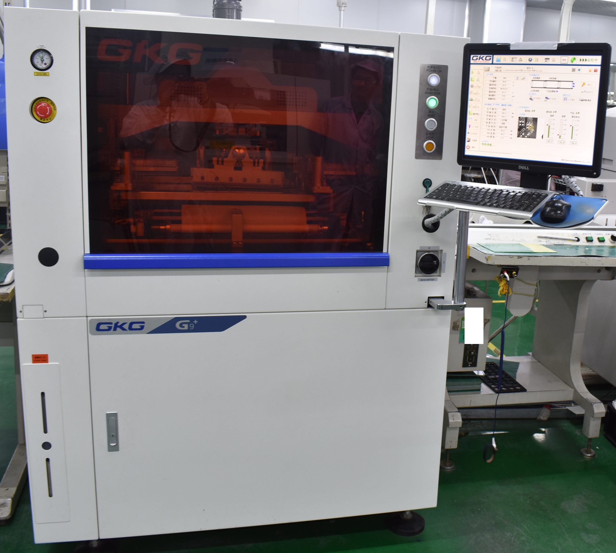
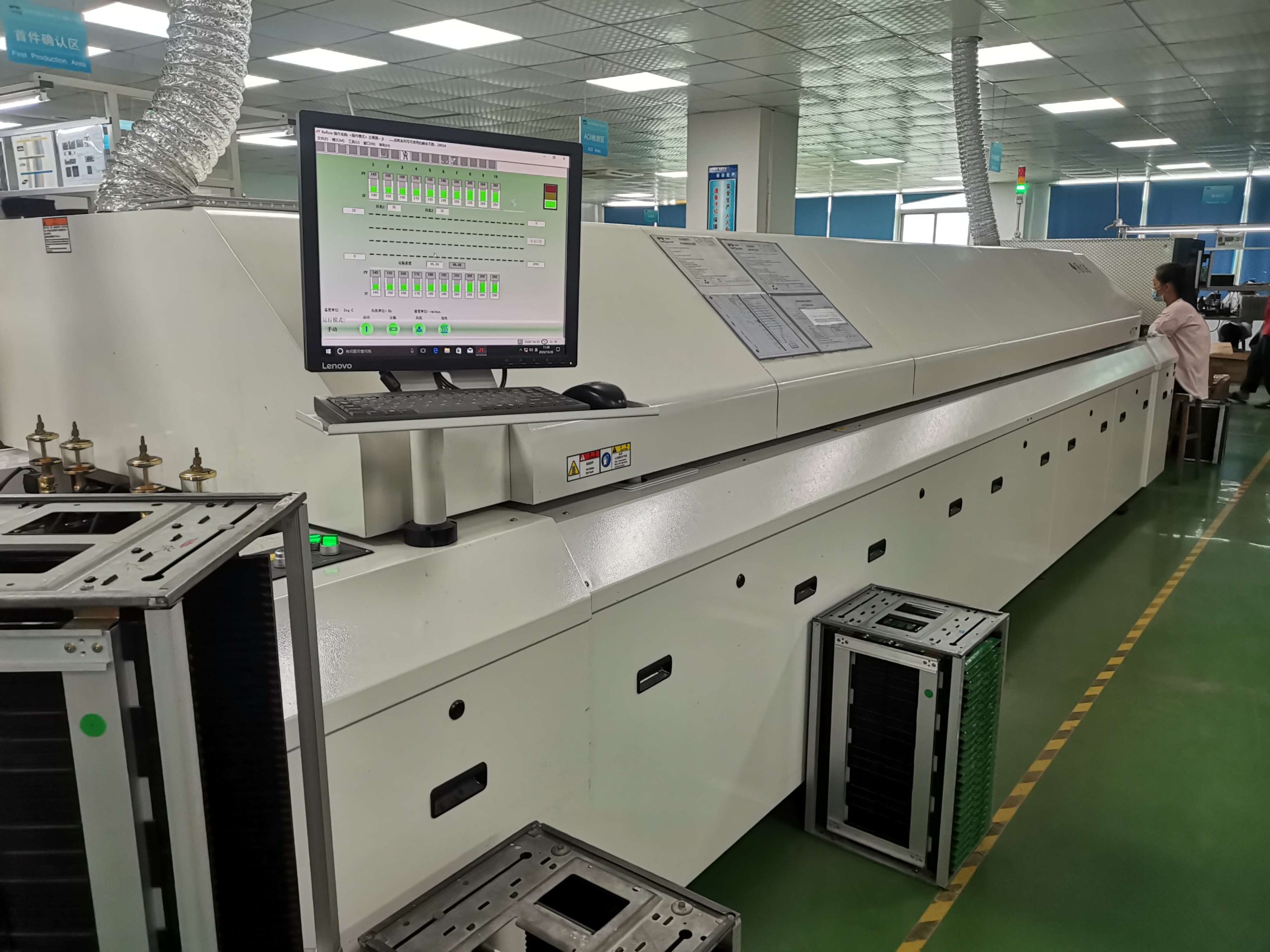
Solder Paste and Stencil Control for Fine-Pitch Assembly
Solder paste and stencil design are where fine-pitch projects succeed or fail. Below 0.4 mm pitch, a paste type that’s fine for a 0.5 mm BGA will bridge across rows, and a stencil aperture that’s 10% too generous will leave you with solder beading you can’t easily rework.
We use Type 5 paste (15–25 µm particle size) for pitch under 0.4 mm and Type 4 for 0.5 mm and up. Stencils are laser-cut stainless steel with electro-polished aperture walls and ±10 µm tolerance — 100 µm thick for sub-0.4 mm parts, 130 µm for 0.5 mm BGA. For QFN thermal pads, we segment the aperture into smaller windows to control solder volume and keep voiding under 25%.
Every board gets 3D solder paste inspection (SPI) right after printing, with paste height held to ±1 µm and target volume held to within ±15%. Anything outside that gets reworked before placement, not after reflow — which is the difference between recovering 30 seconds and rebuilding the board.
Quality, Inspection, and Testing
Every fine-pitch board goes through the same inspection chain so you don’t carry the risk of hidden defects into production:
- 3D solder paste inspection (SPI) after stencil printing — paste height ±1 µm, volume ±15%
- 3D automated optical inspection (AOI) after placement and after reflow — 15 µm lateral, ±5 µm Z resolution
- 5-axis X-ray (AXI) for every BGA, µBGA, QFN, and PoP — 2.5 µm/pixel, IPC 7095 void analysis
- In-circuit test (ICT) and flying probe for boards with limited test point access
- Functional test (FCT) on connectorized outputs — power-up, comms protocol, logic sequence
- IPC-A-610 Class 2 or Class 3 visual inspection by trained operators
- Full traceability by unit barcode — paste lot, stencil ID, oven profile, operator
Defect data feeds back into SPC charts per stencil aperture set, so we catch recurring issues at <500 ppm before they affect your yield.
More PCB Assembly Fabrication Services
Mon-Fri: 24 hours,
Sat: 9am-6pm, GMT+8
Reach us at
[email protected]
24 hours online
+86-199-30589219
Mon-Fri: 24 hours,
Sat: 9am-6pm, GMT+8

