

- PCB Manufacturer
- 10 Layer
10-Layer PCB Manufacturer for Complex Electronic Applications
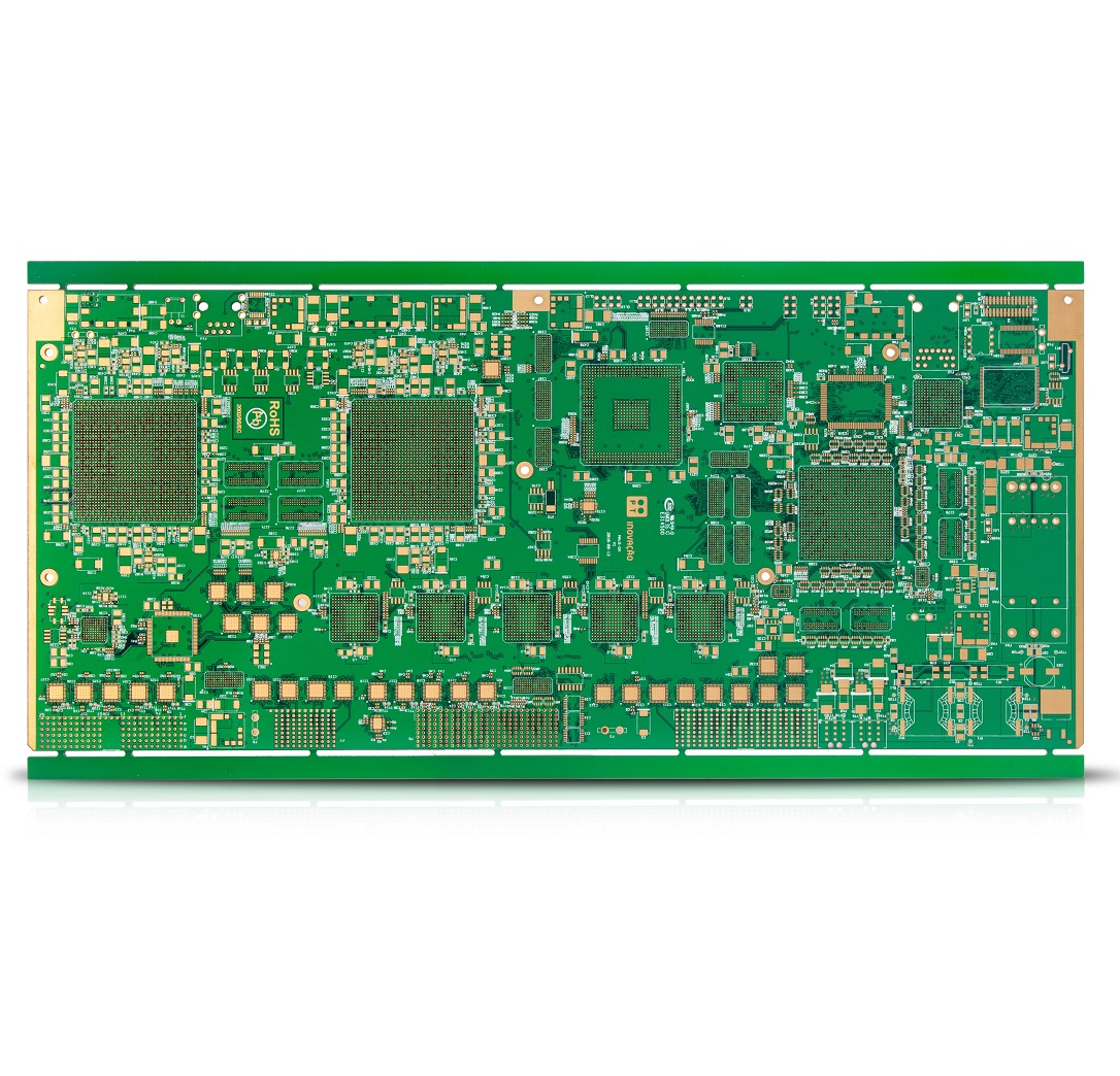
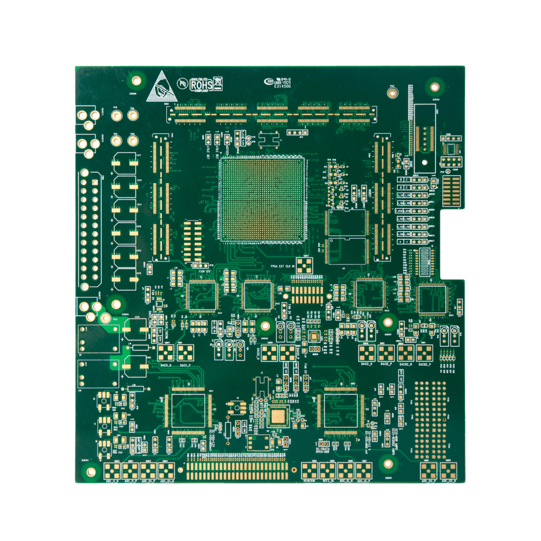
As a trusted 10-layer PCB manufacturer, we design and produce multilayer circuit boards for high-speed signal transmission and space-saving layouts. Some of our clients’ applications include aerospace systems, medical equipment, and advanced telecommunications, where performance and reliability are non-negotiable.


Your Reliable 10-Layer PCB Manufacturer
OurPCB manufactures high-performance 10-layer printed circuit boards with fast prototype turnaround, precise specifications, tighter tolerances, and reliable performance for RF and high-frequency applications. Our specialized manufacturing processes ensure optimal results for your most complex electronic designs.
PCB Manufacturing Process


Our 10-Layer PCB Manufacturing Capabilities
OurPCB manufactures high-performance 10-layer printed circuit boards with precise specifications, tighter tolerances, and reliable performance. This enables us to cater to complex electronic designs such as RF and high-frequency applications. HDI PCB design and manufacturing provide optimized solutions for intricate layer stacking and advanced interconnects.
For a deeper understanding of PCB manufacturing and its various challenges, we offer a comprehensive guide to PCBs, which is ideal for those new to PCB design or looking to expand their knowledge.
High-Density Fabrication for these PCBs involves fine trace capabilities and advanced interconnect options, ensuring that your design not only meets but exceeds performance standards.
- State-of-the-art equipment with ±50μm layer alignment
- Controlled impedance with ±10% tolerance
- High TG FR-4 for thermal stability
- High-Speed & Low-Loss, Polyimide, PTFE, and Rogers HF for advanced applications
- Sophisticated via structures(blind/buried via, microvia)
- Min 2.5 mil fine line capabilities
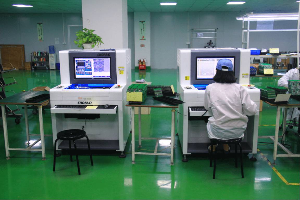
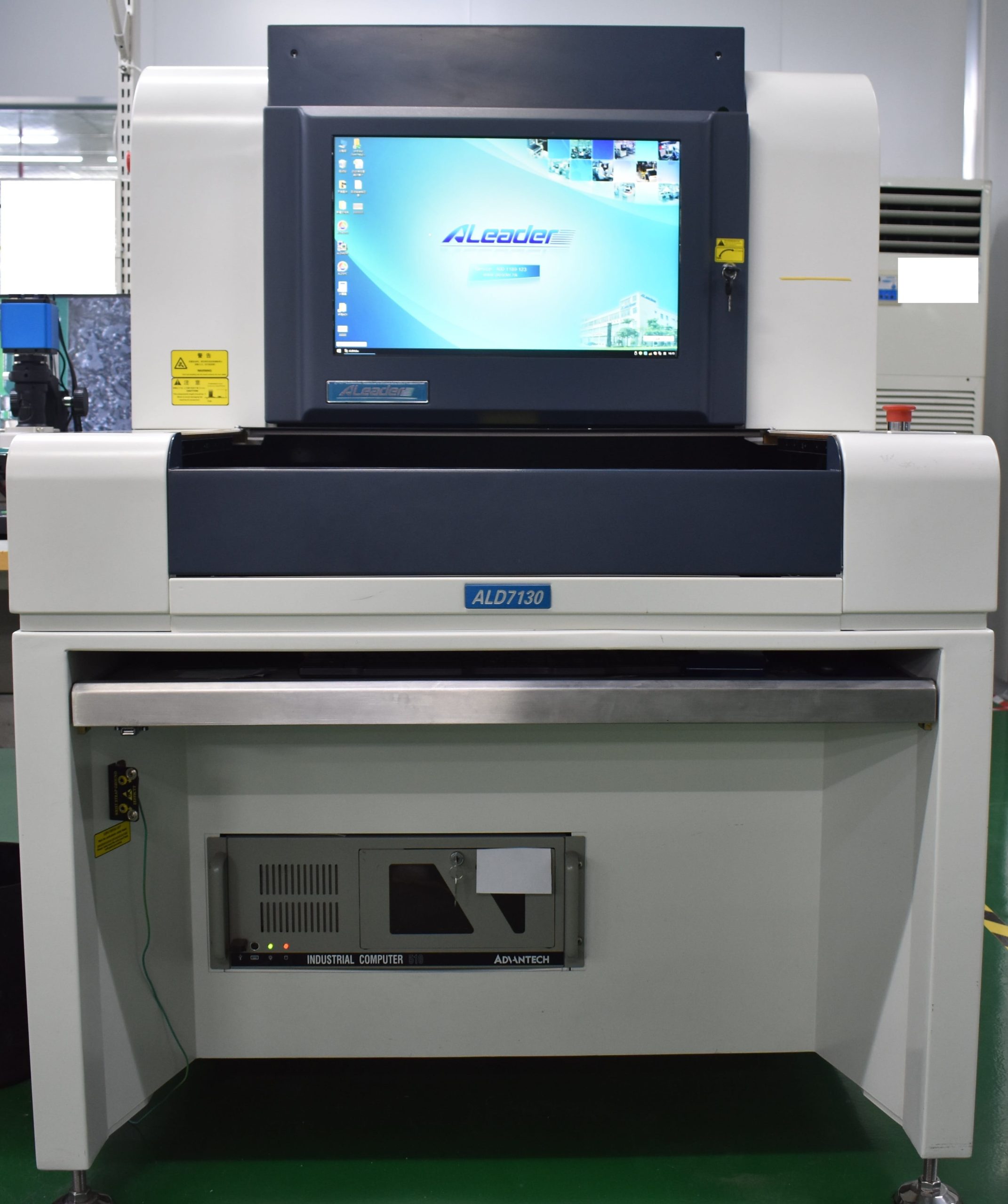
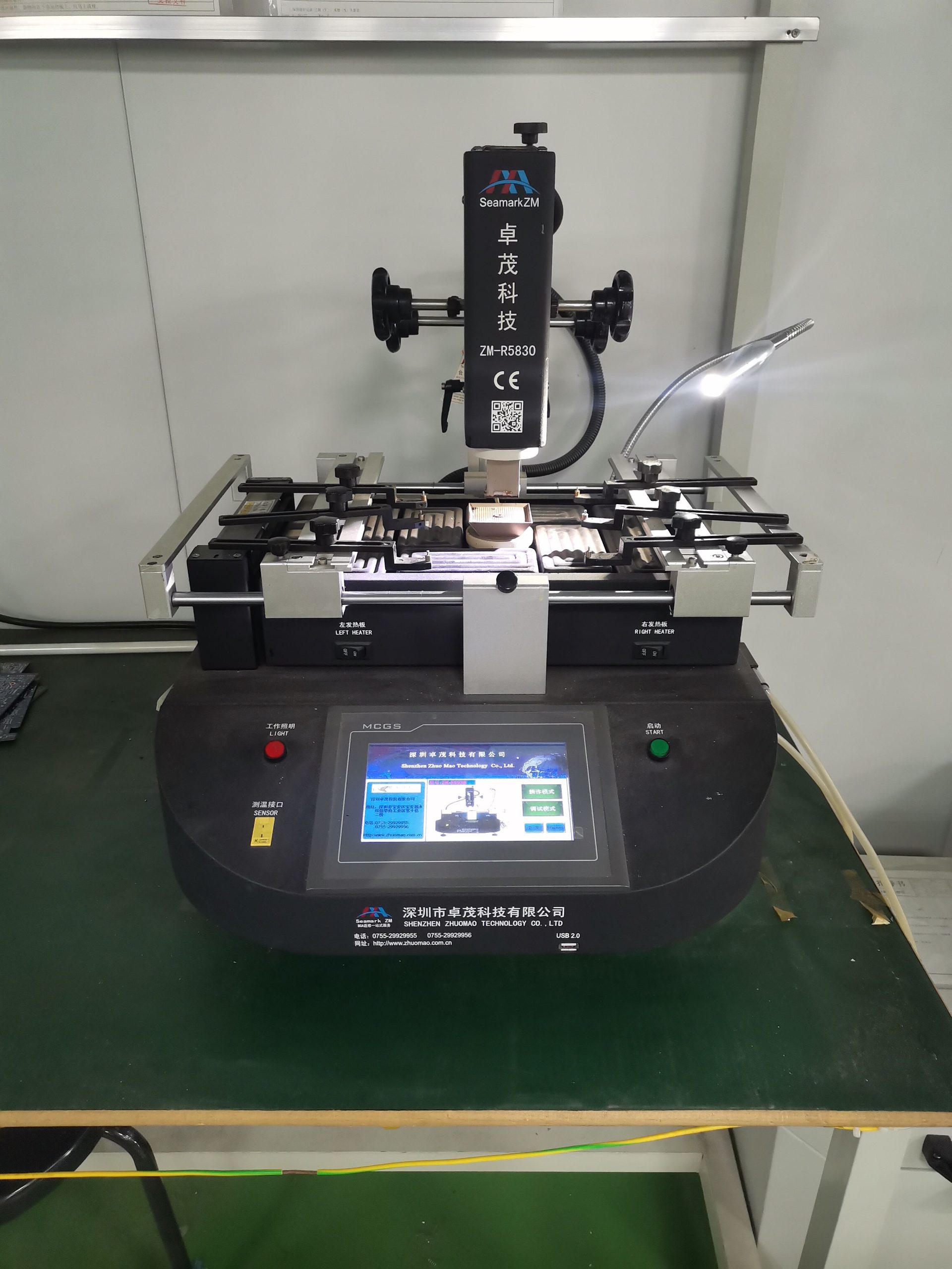
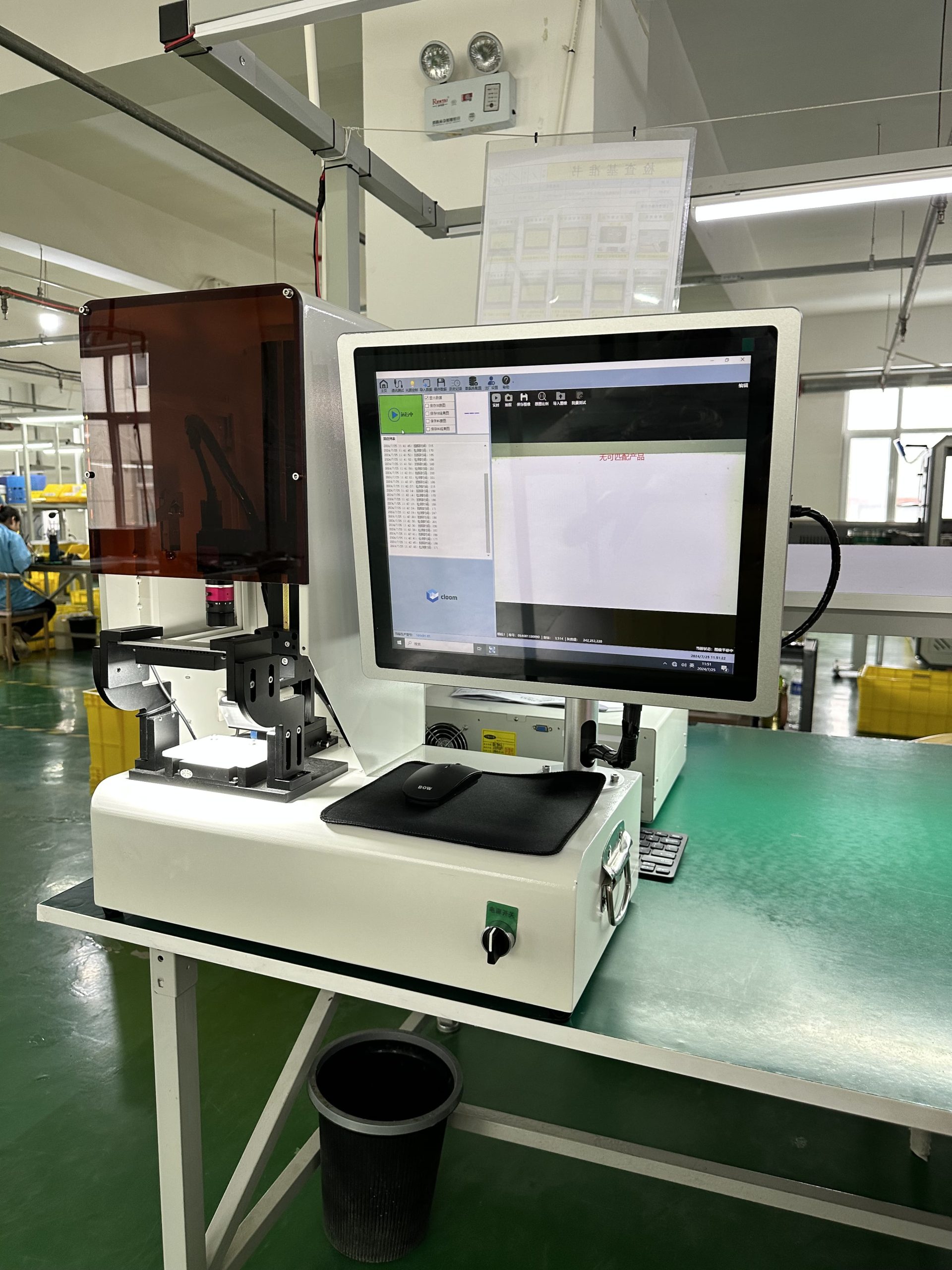
- Advanced AOI inspection
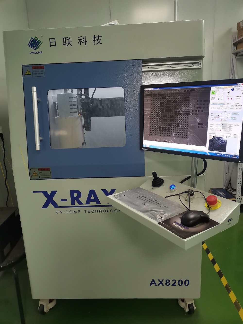
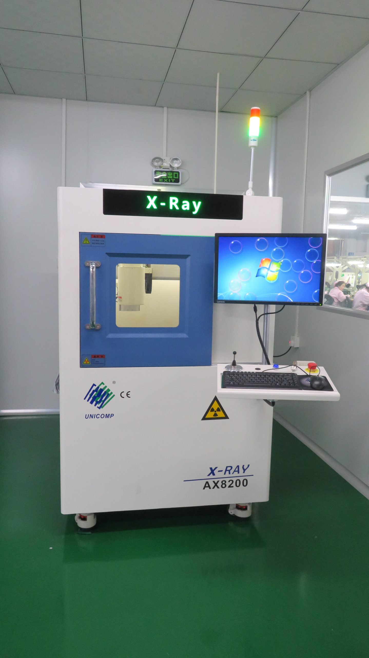
- X-ray verification, ICT test, functional test
Why Choose OurPCB?
We combine advanced technical expertise in PCB fabrication with superior materials and comprehensive quality assurance. For demanding applications, our PCB assembly services include design assistance, advanced production, and thorough testing. Our team works closely with you, ensuring that your design specifications are met with precision.
For anyone looking to avoid common PCB issues like tombstoning or to better understand how schematic diagrams work, we can provide insights into the design and assembly processes.
- ISO 9001, ISO 13485, ISO14001, IATF 16949, and IPC-A-610 Class 2 & 3 certified manufacturing
- Technical support for complex design implementation
- Competitive lead times with scalable capacity
- Complete assembly and testing capabilities
- OurPCB uses premium equipment to manufacture insulated metal substrate PCBs
- Exceptional precision and consistency
- Every IMS board undergoes rigorous testing
- Automated optical inspection (AOI) and thermal analysis
- We design tailored solutions to meet unique project requirements
- OurPCB handles both multilayer and single-sided IMS boards
- Years of experience serving global industries
- OurPCB has a strong reputation as a trusted MCPCB manufacturer
Our 10-Layer PCB Manufacturing Services
- Fine trace capabilities
- Advanced interconnect options
- Application-specific substrate selection
- Thermal management solutions
- Blind/buried vias or microvias
- Controlled dielectric thicknesses
- Full PCBA services
- Original component sourcing
- Electrical performance verification
- Signal integrity validation
- Multiple surface finish options
- Application-appropriate selections

Millions of business and innovators use OurPCB


PCB Board Process
Design (1 day)
- Upload Schematic to Get a Quote
- PCB Review and Quotation
- Customer Makes Payment
- Evaluation & Confirmation of Plan
- Design Start
Layout (1 day)
- Layer Stack-up Design
- Design Rule Setting
- Component Placement Design
- Confirmation & Optimization
- Fanout
Routing (1 day)
- Fanout Optimization
- PCB Routing
- Equal-length Adjustment
- Routing Optimization
- DRC Check
- Routing Confirmation
Optimization (1 day)
- Silkscreen Adjustment
- Data Output
- Customer Final Confirmation
- Production Debugging
- Archiving Projects
- Finish
PCB Board Process
Order Received
- Component Procurement
- Preparation
- PCB Manufacture
- Make Process Flow
Soldering
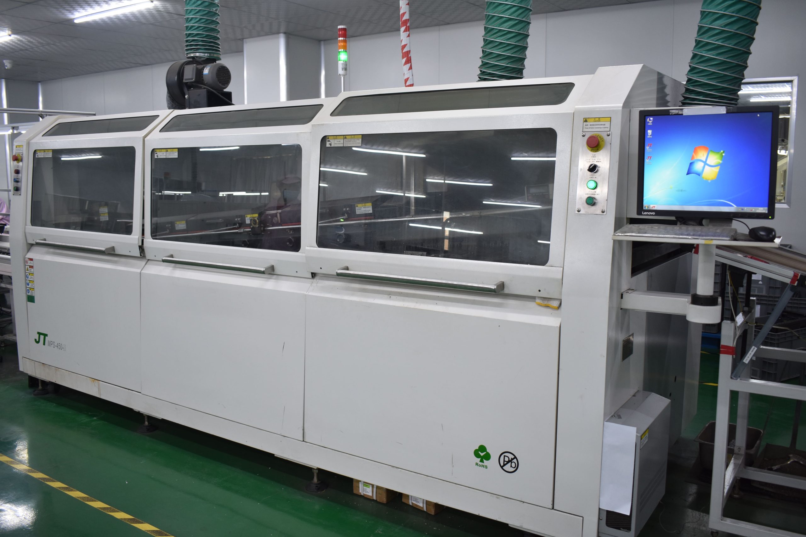
- Solder Printing/Wave Soldering
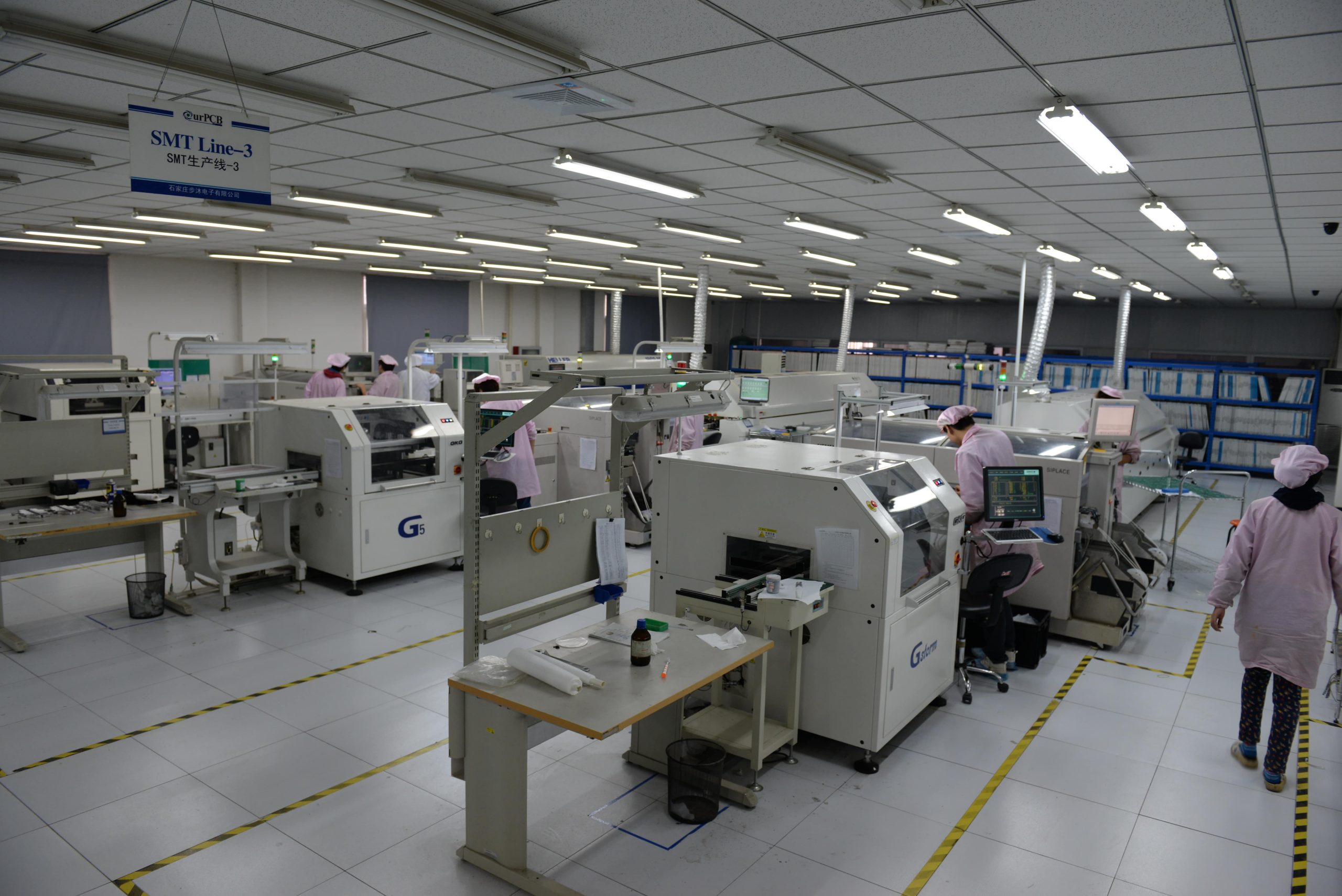
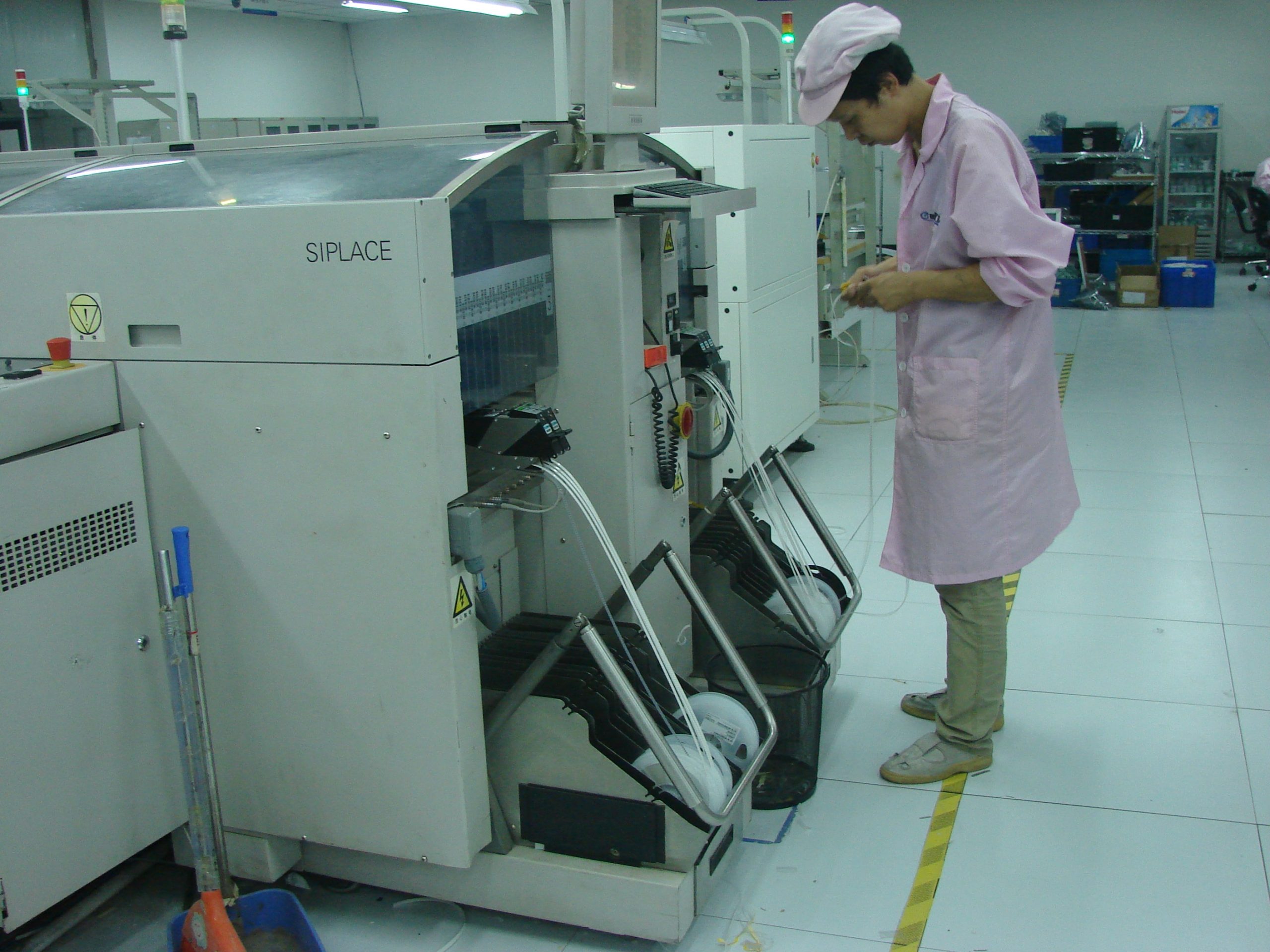
- SMT/Plugging
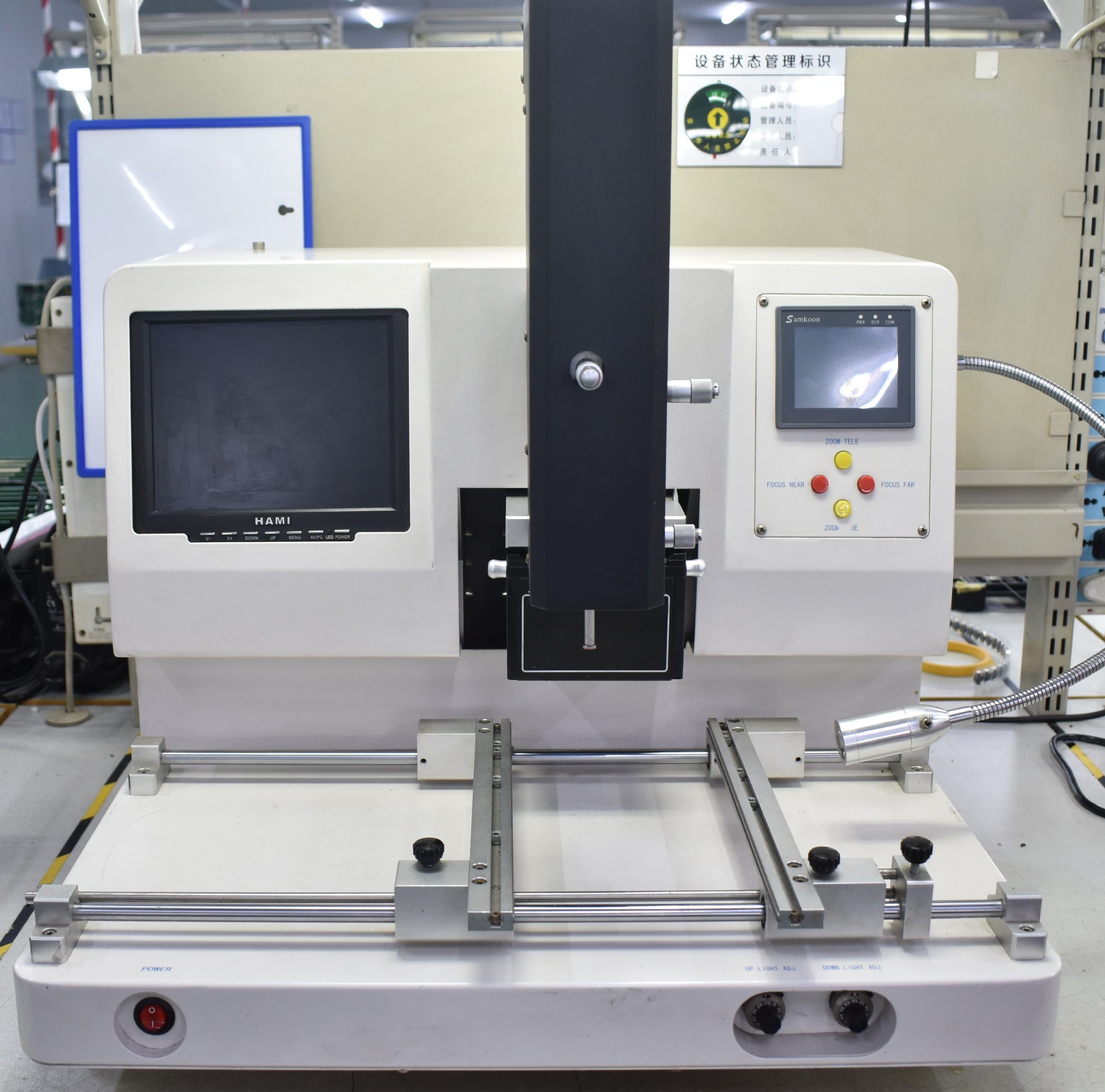
- Inspection (repair if necessary)
- AOI (repair if necessary)
- Transfer
Parts Assembly
- Manual Assembly
- PCBCleaning
- Wire Screw
- Inspection
- Repair If Necessary
Finalization
- Final Confirmation
- Packing
- Shipping
Our Technical Capabilities
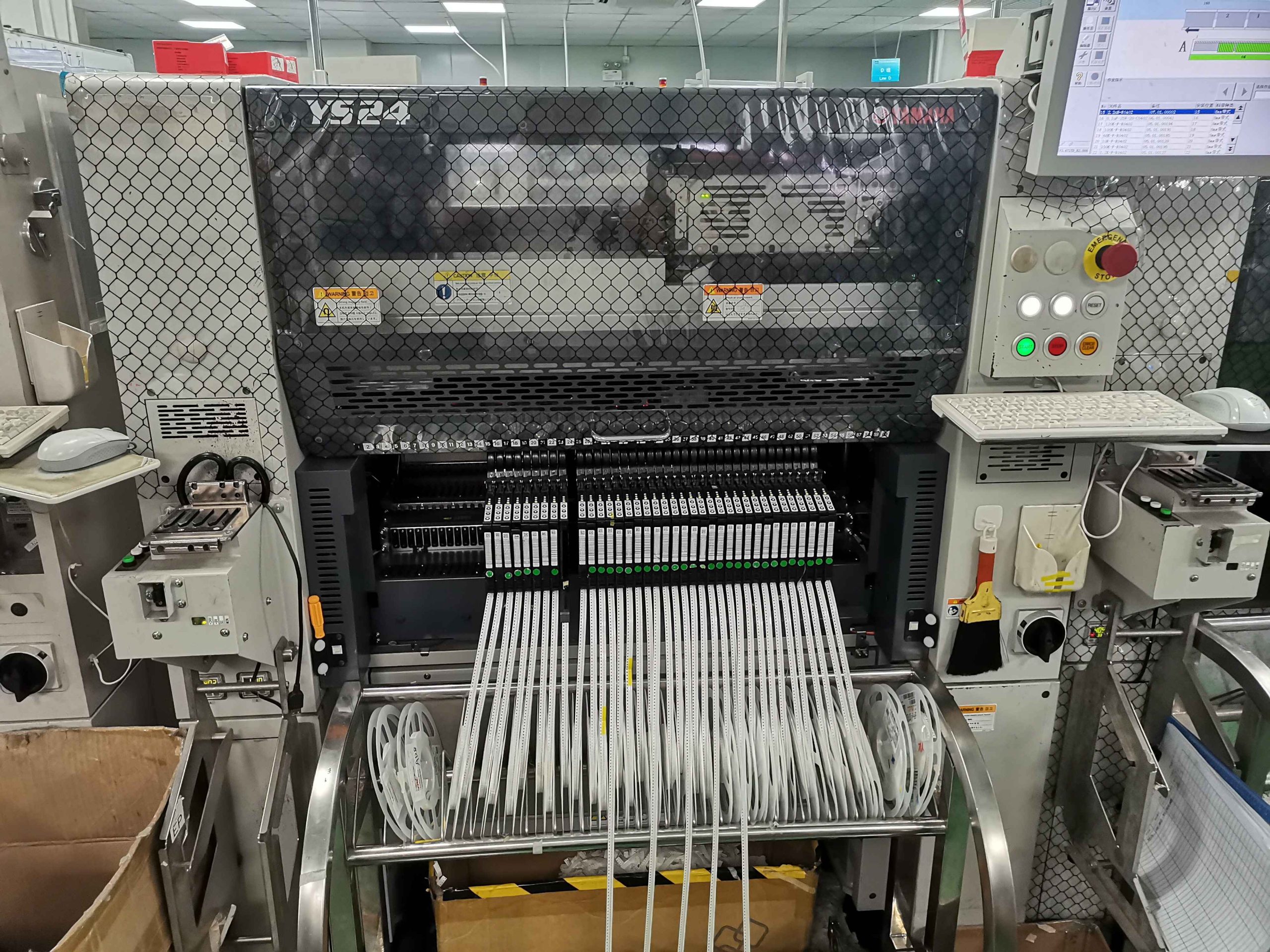
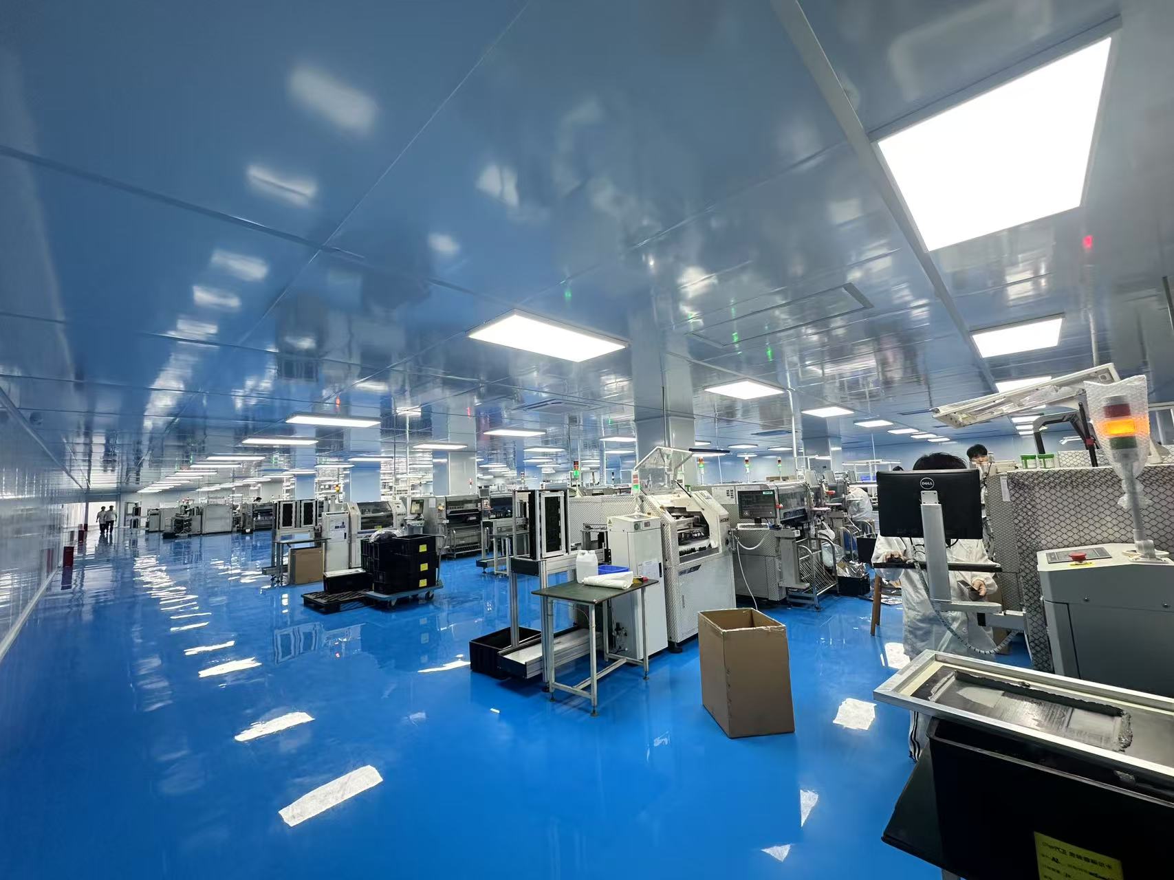
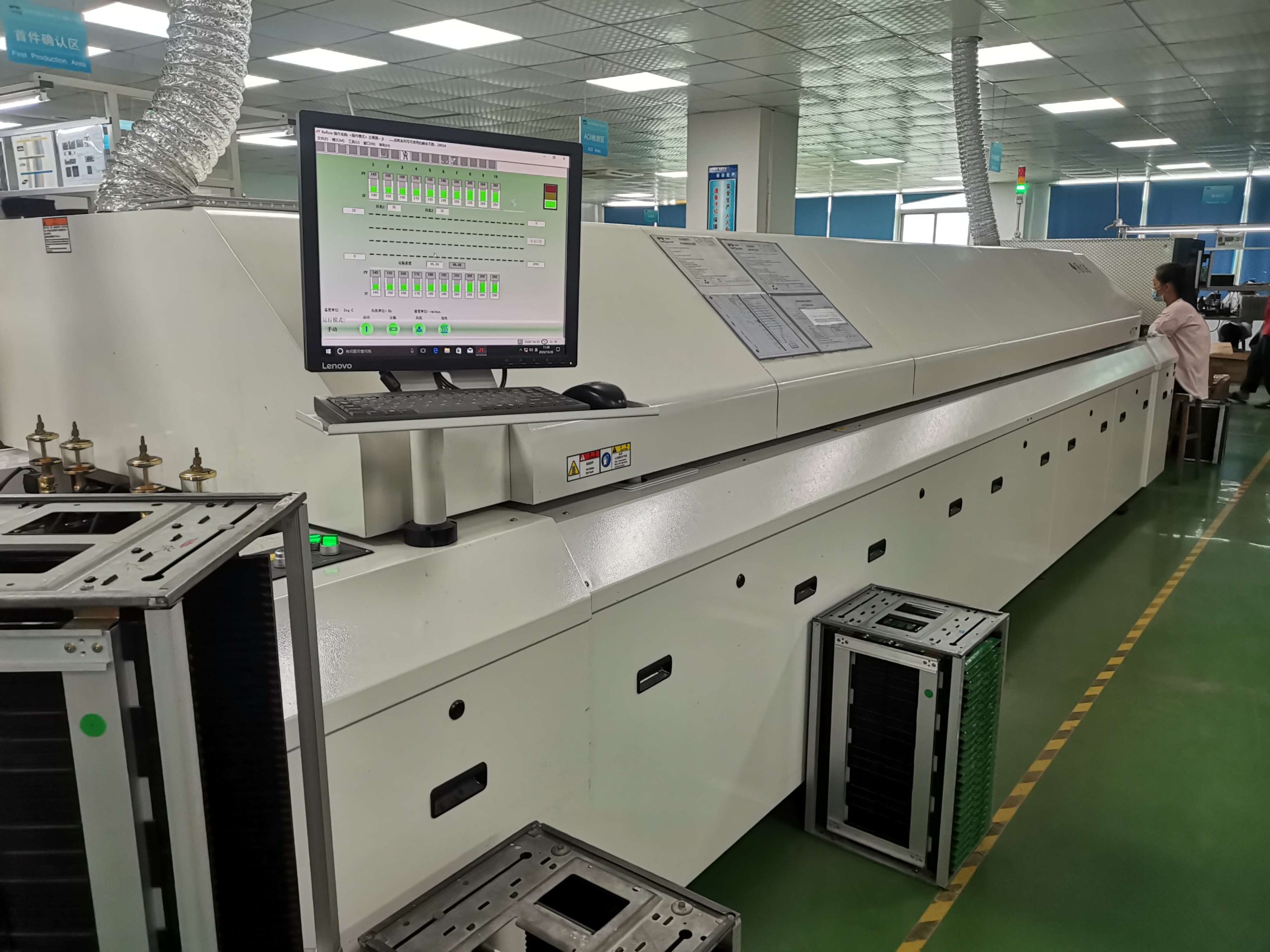
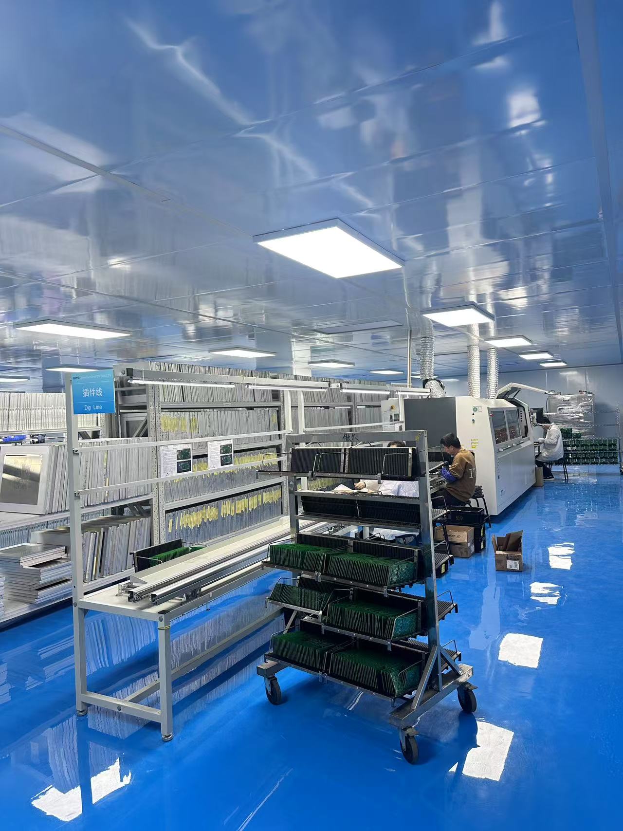
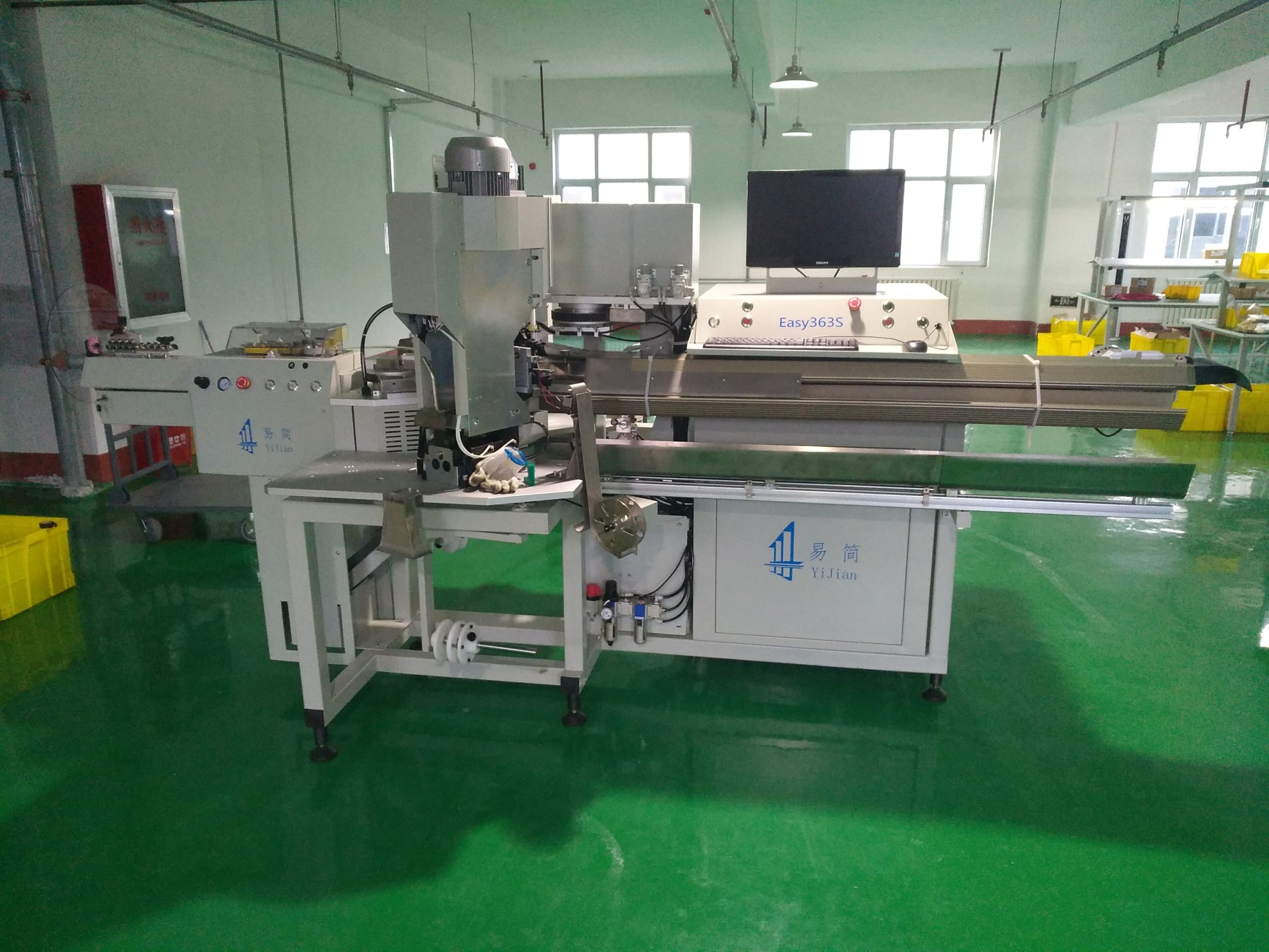
OurPCB uses innovative PCB manufacturing and assembly techniques, including precise registration systems, advanced lamination processes, and multi-stage quality control to ensure consistent performance in all 10-layer PCB stack-ups.
Our Capabilities & Services
- Advanced layer bonding techniques for superior structural integrity
- X-ray and automated optical inspection for internal verification
- Specialized impedance control for high-speed applications
- Comprehensive electrical and functional testing

Mon-Fri: 24 hours,
Sat: 9am-6pm, GMT+8

Reach us at
[email protected]
24 hours online

+86-199-30589219
Mon-Fri: 24 hours,
Sat: 9am-6pm, GMT+8
10 Layer PCB Manufacturer FAQs
What is the lead time for 10-layer PCB manufacturing?
Lead times for 10-layer PCBs depend on the processing area: 8 days for areas <1m², 14 days for 1m² to 3m², 20 days for 3m² to 30m², and 25 days for areas >30m².
What materials do you use for 10-layer PCBs?
For RF (radio frequency) and high-temperature applications in 10-layer PCBs, the most effective materials include Rogers high-frequency laminates (e.g., RO4003C, RO4350B), Teflon/PTFE-based substrates (e.g., Taconic, Arlon), high TG FR-4 (e.g., TG170 or higher), and polyimide.
Can you provide prototype services for 10-layer PCBs?
Yes, we offer comprehensive prototyping services for 10-layer PCBs with expedited timelines and complete testing to validate your design before volume production.
Do you offer assembly services for 10-layer PCBs?
Yes, we provide complete assembly services, including component sourcing, placement, various soldering techniques, and comprehensive testing for fully functional 10-layer PCBAs.
What quality standards do your 10-layer PCBs meet?
Our 10-layer PCBs comply with ISO 9001:2015, ISO 13485:2016, ISO 14001:2015, IATF 16949:2016, and IPC-A-610 Class 2 & 3 standards, ensuring consistent quality and reliability for demanding applications.
What are the challenges in designing a 10-layer PCB?
When designing a 10-layer PCB, it’s important to pay attention to controlled impedance and effective thermal management. Implementing ICT (In-Circuit Testing) during the production phase is one way to enhance PCB production and ensure that your board will meet all necessary requirements.
What are the drawbacks of 10-layer PCBs?
10-layer PCBs offer high performance but come with some drawbacks. They are more expensive to manufacture due to added materials, complex lamination, and tighter tolerances. Design changes are harder to implement once the layout is finalized. Repairs and rework are also difficult because of the dense internal layers. Lastly, lead times are longer compared to simpler boards, especially when custom stack-ups or advanced materials are used.
What is the difference between a PCB and PCBA?
The primary distinction between PCB (Printed Circuit Board) and PCBA (Printed Circuit Board Assembly) is that a PCB is just the bare board, whereas PCBA refers to the entire process where electronic components are mounted, soldered, and tested on the PCB.
For a more in-depth comparison, we’ve provided a detailed breakdown of PCBA vs PCB: Key Differences, so you can understand the nuances between them, especially when dealing with advanced applications like 10-layer designs.
Can I use a 10-layer PCB for timing circuits, such as a 10-minute countdown timer?
Absolutely! 10-layer PCBs can be used in more complex applications, including 10-minute countdown timer circuits, where precise time-keeping and signal integrity are crucial. These designs often require careful layout and controlled impedance to ensure the circuit performs reliably.
Our advanced manufacturing capabilities allow us to create precise, functional designs for all your timing needs. For a deeper understanding of how such circuits are designed, feel free to explore our resources on circuit assembly and related design challenges.
What are the standards that OurPCB follows for 10-layer PCB manufacturing?
OurPCB adheres to ISO certified circuit card assembly standards, ensuring that each board meets the highest levels of quality, reliability, and consistency. Whether you’re looking for high-frequency applications or custom-built designs, our certifications like ISO 9001 and ISO 13485 reflect our commitment to excellence in PCB manufacturing.
For those who want to understand how industry standards affect the manufacturing process, we invite you to dive into Exploring IPC Standards for PCBs, where we break down the key guidelines that govern PCB production and assembly.